Continue to Site

Welcome to EDAboard.com

Welcome to our site! EDAboard.com is an international Electronics Discussion Forum focused on EDA software, circuits, schematics, books, theory, papers, asic, pld, 8051, DSP, Network, RF, Analog Design, PCB, Service Manuals... and a whole lot more! To participate you need to register. Registration is free. Click here to register now.

Input matching shifting of RF power amplifier during measurements

Status
Not open for further replies.

Mabrok

Full Member level 4
Joined
Mar 1, 2017
Messages
223
Helped
0
Reputation
0
Reaction score
1
Trophy points
18
Activity points
1,597
Hi,
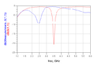
I have design power amplifier using ADS. During the simulation the S11 was good, but after fabricated the design the response was shifted from the original frequency which is 3.5 GHz to 2.5 GHz. what cause this big shifting?
the input matching was aimed to match complex impedance 5+j*1 to 50 ohm. The used matching technique was single quarter wave transformer.

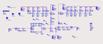
Herewith, i have attached the schematic of my design, measurements & simulation response (red simulation & blue measurements). Thanks in advanced
 

Attachments

  • Schematic.png
    Schematic.png
    28.2 KB · Views: 114
  • Simulation & measurements results.png
    Simulation & measurements results.png
    15.5 KB · Views: 103

Have you ever simulated your PCB Board with Momentum or similar EM Simulator.
This discrepancy is normal because MS Elements in schematic are based on some assumption so their models are not so accurate.In additional to, some unwanted parasitic effects,proximity effects between components,non-ideal/variable substrate parameters etc. impact cumulatively overall response.
You should carefully check PCB Board and implement in regard of this point of view.
Note: Use PDF/PNG Output Feature of ADS in next time because no detail is visible in your schematic.
Look at that, every detail is clearly visible.
sample_png.png

--- Updated ---

Also, there might be some discrepancies between Small Signal s-parameters and Non-Linear model of the transistor.Sometimes, this one may show really serious differences.Don't forget that the Models are mathematical approximate (more or less) representations of the active devices, not themselves.Therefore involving into RF Design Engineering is always difficult.
 
Last edited:
  • Like
Reactions: FvM

    Mabrok

    Points: 2
    Helpful Answer Positive Rating
Have you ever simulated your PCB Board with Momentum or similar EM Simulator.
This discrepancy is normal because MS Elements in schematic are based on some assumption so their models are not so accurate.In additional to, some unwanted parasitic effects,proximity effects between components,non-ideal/variable substrate parameters etc. impact cumulatively overall response.
You should carefully check PCB Board and implement in regard of this point of view.
Note: Use PDF/PNG Output Feature of ADS in next time because no detail is visible in your schematic.
Look at that, every detail is clearly visible.View attachment 164697
--- Updated ---

Also, there might be some discrepancies between Small Signal s-parameters and Non-Linear model of the transistor.Sometimes, this one may show really serious differences.Don't forget that the Models are mathematical approximate (more or less) representations of the active devices, not themselves.Therefore involving into RF Design Engineering is always difficult.
How about the DC blocking caps at the input and output? Does affect the matching as I have used ideal DC block available at ADS under "palette/Lumped-components" which is different from that one used during measurements where i have used Agilent 11742A blocking Capacitor?
 

How about the DC blocking caps at the input and output? Does affect the matching as I have used ideal DC block available at ADS under "palette/Lumped-components" which is different from that one used during measurements where i have used Agilent 11742A blocking Capacitor?
Everything may impact the matching and other specifications.
 

    Mabrok

    Points: 2
    Helpful Answer Positive Rating
Everything may impact the matching and other specifications.
Multilayer Ceramic Capacitors with 100 PF capacitance and 50 VDC which is higher than the voltage that i want to block (28 V)can be used as DC block?
 

Multilayer Ceramic Capacitors with 100 PF capacitance and 50 VDC which is higher than the voltage that i want to block (28 V)can be used as DC block?
No, Collector/Drain Voltage will be higher than Vcc so at 100VDC capacitor should be used to be safe.
 

No, Collector/Drain Voltage will be higher than Vcc so at 100VDC capacitor should be used to be safe.
The transistor is FET, and the applied voltage at the drain side VDS=28 V
 
Last edited:

Have you ever simulated your PCB Board with Momentum or similar EM Simulator.
This discrepancy is normal because MS Elements in schematic are based on some assumption so their models are not so accurate.In additional to, some unwanted parasitic effects,proximity effects between components,non-ideal/variable substrate parameters etc. impact cumulatively overall response.
You should carefully check PCB Board and implement in regard of this point of view.
Note: Use PDF/PNG Output Feature of ADS in next time because no detail is visible in your schematic.
Look at that, every detail is clearly visible.View attachment 164697
--- Updated ---

Also, there might be some discrepancies between Small Signal s-parameters and Non-Linear model of the transistor.Sometimes, this one may show really serious differences.Don't forget that the Models are mathematical approximate (more or less) representations of the active devices, not themselves.Therefore involving into RF Design Engineering is always difficult.

How about the effect of transistor's parasitic capacitance ?
 

How about the effect of transistor's parasitic capacitance ?
Model of a transistor should normally contain all necessary (intrinsic and extrinsic) elements but some models may not have package parasitic components.You have to find or extract those elements if they are not negligible at all.In roder to find such elements, there are some either package extractors based on analytically pre-defined elements or straightforward 3D EM simulators.
 

Model of a transistor should normally contain all necessary (intrinsic and extrinsic) elements but some models may not have package parasitic components.You have to find or extract those elements if they are not negligible at all. In roder to find such elements, there are some either package extractors based on analytically pre-defined elements or straightforward 3D EM simulators.
The values of these capacitors already available in the datasheet. So, how to off rid from their effects on the impedance matching?
 

Status
Not open for further replies.

Part and Inventory Search

Welcome to EDABoard.com

Sponsor

Back
Top