stevenv07
Member level 2
Hello everyone,
I have a problem as follows:
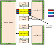
My chip is analog hard macro dominant as shown in the attached figure. I/Os for analog hard macro have been implemented. The digital part is put at almost middle of the chip. It is difficult to place the I/O PAD for signals and power/ground at the IO AREA of the chip. So, my question is:
Can I implement the I/O PAD around the digital part, and consider it as a hard macro, them place it in the chip? then we can connect bumps to those I/O pads at top-level? See the attached figure for detail.
Many thank
Steve.
I have a problem as follows:
My chip is analog hard macro dominant as shown in the attached figure. I/Os for analog hard macro have been implemented. The digital part is put at almost middle of the chip. It is difficult to place the I/O PAD for signals and power/ground at the IO AREA of the chip. So, my question is:
Can I implement the I/O PAD around the digital part, and consider it as a hard macro, them place it in the chip? then we can connect bumps to those I/O pads at top-level? See the attached figure for detail.
Many thank
Steve.