mayjailomo
Newbie level 5
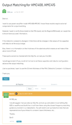
Hi all,
I am new to this field. I am now drawing a PCB for a power amplifier (HMC408). Although analog device has provided the reference schematic and PCB layout, external matching circuit is required for this IC, and the matching circuit in the reference design is designated for RO4350 and CPWG while I am using other substrate and another type of transmission line (microstrip line).
I have searched in google and someone suggested to use the s2p file (they said that the s2p file is for the IC, not for the eval board) provided by analog device to do the impedance matching in ADS. I have tried it on ADS but I found that the S11 and S21 is pretty good and matched with the data provided in the datasheet even when I simply connected the 2 ports with 2 50Ohm terms. When I connected the s2p output port to the external matching components suggested from the datasheet, the performance dropped. May I ask if that's normal? Can I really do the impedance matching using the s2p file provided by analog device?
I am sorry for my poor english.
Many thanks!
Reference schematic for HMC408:

Setup in ADS: ( The parameters of the CPWG are measured from the gerber file provided by analog device)

S11, S21: (connected to the terms directly)

s11,s21 with external matching circuit:

I am new to this field. I am now drawing a PCB for a power amplifier (HMC408). Although analog device has provided the reference schematic and PCB layout, external matching circuit is required for this IC, and the matching circuit in the reference design is designated for RO4350 and CPWG while I am using other substrate and another type of transmission line (microstrip line).
I have searched in google and someone suggested to use the s2p file (they said that the s2p file is for the IC, not for the eval board) provided by analog device to do the impedance matching in ADS. I have tried it on ADS but I found that the S11 and S21 is pretty good and matched with the data provided in the datasheet even when I simply connected the 2 ports with 2 50Ohm terms. When I connected the s2p output port to the external matching components suggested from the datasheet, the performance dropped. May I ask if that's normal? Can I really do the impedance matching using the s2p file provided by analog device?
I am sorry for my poor english.
Many thanks!
Reference schematic for HMC408:
Setup in ADS: ( The parameters of the CPWG are measured from the gerber file provided by analog device)
S11, S21: (connected to the terms directly)
s11,s21 with external matching circuit: