Continue to Site

Welcome to EDAboard.com

Welcome to our site! EDAboard.com is an international Electronics Discussion Forum focused on EDA software, circuits, schematics, books, theory, papers, asic, pld, 8051, DSP, Network, RF, Analog Design, PCB, Service Manuals... and a whole lot more! To participate you need to register. Registration is free. Click here to register now.

I need to design a coaxial balun for 2.4GHz application.

Status
Not open for further replies.

robismyname

Full Member level 6
Full Member level 6
Joined
Jan 17, 2008
Messages
390
Helped
11
Reputation
22
Reaction score
9
Trophy points
1,298
Location
Central Florida
Activity points
4,603
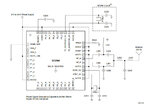
I have a test board that has a TI reference design for a Lattice type balun (see attached). The lattice balun on one side is assumed to be matched to the cc2540 at 70 +30j (obtained from TI's spec sheet). And the other side of the lattice balun is assumed to be matched to 50 ohms (obtained from TI's spec sheet).

What I want to do is measure the impedance of the TI referenced design lattice balun on the differential side for now but the problem is that my VNA does not support differential inputs.

Since my VNA does not support differential inputs I need to make a coaxial balun that allows me to connect the differential side of the TI reference design lattice balun that exist on my test board.


So my questions are:

1) How do I design a coaxial balun for 2.4GHz applications? Any notes, application notes, white papers, links, calculators available that are good resources that can help me with this design?

2) Will the coaxial balun convert from differential to single ended without changing the assumed differential impedance of 70+30j? Or will the coaxial balun change my impedance on the differential side from 70+30j to 50 ohms?

3) Is it feasible/possible to connect my TI reference design test board that has the Lattice type balun on it to my vna through the coax balun without changing the assumed impedance of 70+30j?

4) Is my approach ok?
 

Attachments

  • cc 2540 balun.jpg
    cc 2540 balun.jpg
    102.5 KB · Views: 103
  • cc2540.pdf
    657.4 KB · Views: 93
Last edited:

I believe that your intended measurement setup will involve a larger error than the possible impedance matching error with the suggested LC balun.

It makes more sense to verify the PA output impedance at the 50 ohm side, preferably by load pulling.

The balun can be measured most accurately as a single ended three-port measurement. It's basically possible with a standard VNA by switching the ports sequentially. The results can be transformed to get differential S-parameters.
 

I believe that your intended measurement setup will involve a larger error than the possible impedance matching error with the suggested LC balun.

As an alternate solution can i just make another board that has the cc2540 connected to the LC balun on the differential side using a known output power? and then measure the output powe on the single side? If the output power loss is significant then that means I have a matching issue? Please advise

It makes more sense to verify the PA output impedance at the 50 ohm side, preferably by load pulling.
The balun can be measured most accurately as a single ended three-port measurement. It's basically possible with a standard VNA by switching the ports sequentially. The results can be transformed to get differential S-parameters.

so with this three port measurement:

1) how will I connect my board that has the LC balun on it to a VNA?
2) switching the ports sequentially requires a mechanical switch or toggling the buttons on the VNA? How would you apply the switching to the test. Need better explanation.
3) Can you provide an example of what the results would be and how would you transform it to get differential parameters?
4) Exactly why are some transceiver IC's differential and others are single? Is one better than the other? What does it mean to have RF signal come out of a IC (2540) as differential?

Please advise.
 

Measuring transceiver output power, e.g. with a SA is the most simple method to verify the matching network, load pulling (varying the complex load impedance until maximum output power is achieved) the next step. In case of a differential output, it can't compensate for a balun phase error, however.

Q1. Depends on. PA impedance measurement during send phase is possible with restrictions. Presumed that the VNA can handle the transceiver output power, it need to be triggered to send phase. Impedance can be measurement with some distance to carrier only.

Q2-Q3 are related to general VNA practice. Ports can be also switched by reconnecting cables, you don't necessarily need a mechanical or automated switch. Single ended to differential S-parameter transformation has been repeatedly discussed at edaboard. With most standard VNAs the calculation has to be performed by an externaltool, e.g. a spreadsheet calculator.

Q4 is a matter of RF chip design. Differential output is usually better for low voltage, also promises better attenuation of harmonics and spurs by balun common mode supression.
 

1. you could make the balun with just one inch of 50 ohm coax cable. at one side shield and center wire is the differential input and other side the center wire is single ended output if the shield is connected to ground. it is a simple transmition line transformer. it is recommended to use the thinnest coaxial cable available to reduce parasitic effects.
2. coaxial balun does not match complex impedance to real one. extra matching circuit is necessary.
3. diff amplifiers have better linearity, less 2nd harmonic, and higher power handling and suitable for integrated circuit design but they need balun. in some designs external baluns is used and in others internal integrated balun is used which is made with planar magnetically coupled inductors. these integrated transformer has lower efficiency due to substrate loss and higher spur/noise due to substrate coupling.
4.the output impedance of the amplifier is not the value which is determined in datasheets. the value in datasheet is simply optimal value of load for highest gain and efficiency so generally you could not connect VNA to the amplifier to measure its output impedance. the impedance is determined by load pulling.

BEST.
 

You can ask the vendor for S parameters.
 

Status
Not open for further replies.

Part and Inventory Search

Welcome to EDABoard.com

Sponsor

Back
Top