Tahirmis_ic
Junior Member level 1
Hi all,
The question is about the soft clipping stage of an oscillator integrated circuit designed with Cadence Virtuoso. The technology used is CMOS and the process is AMS 0.35um.
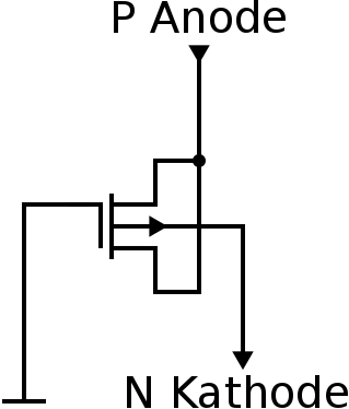
I want to design a back to back silicon diodes in the negative feeback path of an op-amp in CMOS technology. The process design kit used offers a lateral bjt and vertical bjt as pn junctions solution.
In the case of vertical bjt (Emitter P+, Base Nwell, Collector PSub), the fact that diodes are in the feedback path of my op-amp doesn't allow to connect Base to Collector, since collector is connected to Substrat. Is it right (Nwell Psub process) ?
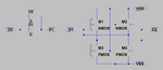
My lateral bjt transitor consists of a vertical and a lateral part. Emitter and Collector are separated by the gate. How to connect the gate? to Base ? Is the lateral bjt a better solution than the vertical bjt to implement my back to back silicon signal diodes? Why?
I think we can't implement the back to back diode behavior with mosfets connected as a diode in the case of negative feeback path of an op-amp . It is right?
Because I am using Nwell Psub process. In the case of the pmosfet transistor, bulk is Nwell and it is connected to the higher voltage in the circuit, but I can connect it to a level less than Vdd because we have several nwells and we mustnt connect them to common voltage, so they could be connected to different voltages. In the case of nmos, the bulk is Psub, and I should connect it to Vss (knowing that there is only one substrat, it is right?). This why I said that implementing a back to back silicon diodes in the negative feeback path of an op-amp in CMOS technology is not allowed whith the mosfet configured as diode with the process used. Am I right?
I want to know if there are others possibilities than using paratic pnp to implement a back to back diodes in cmos technology with Nwell Psub process ? Actualy I use the Base Emitter junction and I connect Collector to VSS because The process used doesn't allow me to connect in a other way.
Thanks all,
The question is about the soft clipping stage of an oscillator integrated circuit designed with Cadence Virtuoso. The technology used is CMOS and the process is AMS 0.35um.
I want to design a back to back silicon diodes in the negative feeback path of an op-amp in CMOS technology. The process design kit used offers a lateral bjt and vertical bjt as pn junctions solution.
In the case of vertical bjt (Emitter P+, Base Nwell, Collector PSub), the fact that diodes are in the feedback path of my op-amp doesn't allow to connect Base to Collector, since collector is connected to Substrat. Is it right (Nwell Psub process) ?
My lateral bjt transitor consists of a vertical and a lateral part. Emitter and Collector are separated by the gate. How to connect the gate? to Base ? Is the lateral bjt a better solution than the vertical bjt to implement my back to back silicon signal diodes? Why?
I think we can't implement the back to back diode behavior with mosfets connected as a diode in the case of negative feeback path of an op-amp . It is right?
Because I am using Nwell Psub process. In the case of the pmosfet transistor, bulk is Nwell and it is connected to the higher voltage in the circuit, but I can connect it to a level less than Vdd because we have several nwells and we mustnt connect them to common voltage, so they could be connected to different voltages. In the case of nmos, the bulk is Psub, and I should connect it to Vss (knowing that there is only one substrat, it is right?). This why I said that implementing a back to back silicon diodes in the negative feeback path of an op-amp in CMOS technology is not allowed whith the mosfet configured as diode with the process used. Am I right?
I want to know if there are others possibilities than using paratic pnp to implement a back to back diodes in cmos technology with Nwell Psub process ? Actualy I use the Base Emitter junction and I connect Collector to VSS because The process used doesn't allow me to connect in a other way.
Thanks all,