Continue to Site

Welcome to EDAboard.com

Welcome to our site! EDAboard.com is an international Electronics Discussion Forum focused on EDA software, circuits, schematics, books, theory, papers, asic, pld, 8051, DSP, Network, RF, Analog Design, PCB, Service Manuals... and a whole lot more! To participate you need to register. Registration is free. Click here to register now.

How to drive a transistor into saturation in cadence (if its in triode)?

Status
Not open for further replies.

Khisha

Newbie level 2
Joined
Aug 24, 2011
Messages
2
Helped
0
Reputation
0
Reaction score
0
Trophy points
1,281
Activity points
1,317
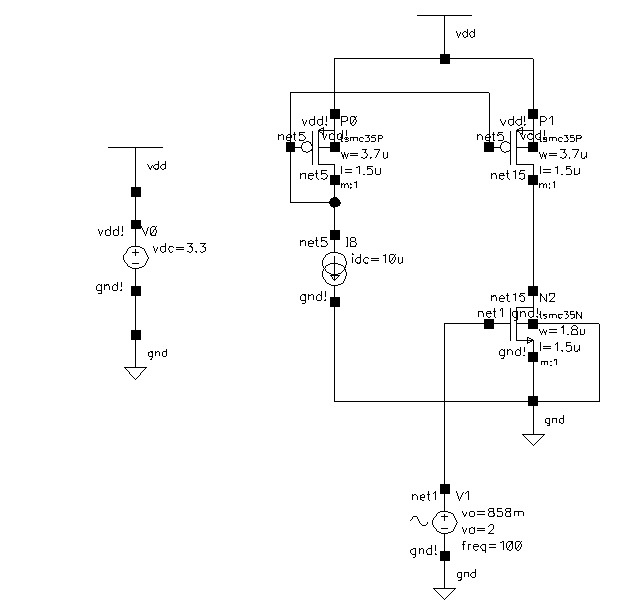
I am a newbie in both analog design and cadence. I'm having problem while simulating this simple single stage CS amplifier as shown in the diagram. Here, P1 is in saturation but N2 isn't. How can I drive N2 into saturation also. Please suggest me, what parameters should I play with.


The transistor N2 operates in saturation if and only if Vgs2 - Vtn <= Vds2, it means that Vg2 - Vd2 <= Vtn, Base on your lib, you can calculate the range of Vd2 (= Vd1) then you can set the value of Vg2 to ensure Vg2 - Vd2 <= Vtn.
Regard.
 

... How can I drive N2 into saturation also.

If V0=2V is the DC part of V1, this is much too large, should be in the order of Vth(N2)+Veff. Working with an inversion coefficient IC = 30 .. 50 , Veff ≈ 450..550mV .

Also, the ac part of V1, vo=858m is too large, I think. It overdrives N2.
 
Last edited:

Thanks ducvilla and erikl. Really appreciate your time. How can I control the drop Vsd of P1 in the figure (i.e. manipulating W/L or Vgs) or across a transistor in general?
 

Transistors P0,P1 form a simple 1:1 pmos current mirror.So,in this case you have the following ways to affect Vds os P1 :

1.)Varying the Ibias of the ideal current source,consequently you will manipulate Vgs as you said.
2.)Manipulating the W,L of the transistors that form the mirror.
3.)Changing the V1 DC potential.
4.)Changing the W,L of transistor N2.

If you have a simulator available,try to put things on a schematic and start playing with respect to the basic equations that describe the circuit.

Notice : The bulk node of nmos devices should be connected to the substrate global network (generally sub!) and not to gnd!In any case,for simple circuits and education purposes you can live with the connection you already have.
 
  • Like
Reactions: Khisha

    Khisha

    Points: 2
    Helpful Answer Positive Rating
If you're new to analog design it is time to understand one thing. When you have two transistors like in you figure connected with their drains (P1 and N1) it is practically impossible to maintain them in saturation just by sizing the transistors or choosing the current. Depending on the gain of the amplifier any small mismatch in the currents each of the transistors wants to source/sink will drive one or the other in triode mode. In simulation you can always find a gate voltage for N1 for example that keeps both in saturation but this is not practical for real circuits - it may work in one process corner but will fail in another. There should be some feedback mechanism that adjusts the dc gate voltage of N1 or the DC current of P1 such that the output voltage (the common drains connection) has a value, such that both the pmos and nmos are in saturation.
 
  • Like
Reactions: Khisha

    Khisha

    Points: 2
    Helpful Answer Positive Rating
Dear Khisha
Hi
I should say an important thing to you about saturation region:
In mosfets: when VGS become near 15 volts , your mosfet will work in saturation region . and about IGBT s too(GE =15) . and about BJT s : when BE voltage become 0.6 volt for silicon ( with enough base current) your BJT will work in saturation region.
About J fet= when VGS = Zero ( n type) your current will be IDSS ( will saturate )
Best wishes
Goldsmith
 

A small difference is that what is called saturation in bjt is not the same thing in mos


Dear Khisha
Hi
I should say an important thing to you about saturation region:
In mosfets: when VGS become near 15 volts , your mosfet will work in saturation region . and about IGBT s too(GE =15) . and about BJT s : when BE voltage become 0.6 volt for silicon ( with enough base current) your BJT will work in saturation region.
About J fet= when VGS = Zero ( n type) your current will be IDSS ( will saturate )
Best wishes
Goldsmith
 

Dear sutapanaki
Hi
In mos when the GS become short circuit , you can say that the mosfet is saturated. and in bjt s , if CE junction become short circuit , you can say that the BJT is saturated. here , my mean by short circuit , is not that the elements become destroy my mean is that their performance as a simple switch.
All the best
Goldsmith
 

No, I didn't mean to say that the devices would be destroyed. What I meant was that for the bjt to be in saturation we need the base higher than ~0.6V compared to the collector. Then Vce is small, 0.2v or maybe lower (at least for integrated bjts). The transistor can be viewed as a closed switch in this mode. In the case of the MOS transistor, you don't make GS short. Similar to the bjt, if you have the gate higher than the drain by one threshold or more, than the transistor enters into its ohmic region and Vds can really become very close to 0V depending on the current. But this mode of operation for mos transistors is not called saturation, rather this is the triode regime. When drain voltage is such that Vgs-Vth<Vds and the mos device works as current source, then we usually say that the transistor is in saturation.

Dear sutapanaki
Hi
In mos when the GS become short circuit , you can say that the mosfet is saturated. and in bjt s , if CE junction become short circuit , you can say that the BJT is saturated. here , my mean by short circuit , is not that the elements become destroy my mean is that their performance as a simple switch.
All the best
Goldsmith
 

Dear sutapanaki
Again Hi
When the be voltage become one volt , you can be ensure that the BJT IS on see here:
bjt2.JPGbjt.JPG
Kind Regards
Goldsmith
 

What I meant was that for the bjt to be in saturation we need the base higher than ~0.6V compared to the collector.
... compared to the emitter, you mean, of course.
 

No, I really mean compared to the collector. When base is 0.6v (or more) higher than collector, the collector-base junction is forward biased (and of course the BE junction is also forward biased) and the bjt is in saturation (talking about npn). If BC junction is reverse biased, the bjt is in the active region of operation i.e. current source kind of operation.
Goldsmith, if base is 1V and collector is less than 9.4V, then yes, it is in saturation. But let me ask you this - what is the operation region of that bjt if Vb=1V and Vc=1V - assume there is no voltage drop in the internal collector resistance and that the BE junction can sustain 1v across it?
 

Dear sutapanaki
Hi
No if Vbe =1v and vc =1v we can not say that bjt is in saturation , i think. but when we say that the bjt is in saturation , actually be is in forward bias and bc is in reverse bias .
Best Regards
Goldsmith
 

Can't agree. Unless we clarify the polarities. Are you saying that when base is more positive (by 0.6 and more) than emitter and when collector is more positive than the base, the transistor is in saturation?
 

Dear sutapanaki
Hi
see my post that in that i attached a circuit. you can see thing that i said in that.
Best Wishes
Goldsmith
 

That's really not what one would understand as BJT saturation :roll:

Then can you please explain what is understood when we say the bjt is in saturation and what when said it is in active region?
 
Last edited:

Then can you please explain what is understood when we say the bjt is saturation and what when said it is in active region?

All questions related with these transistor properties have been discussed extensively in this forum before.
In this context it is to be noted that - because of historical reasons - there are two different saturation region definitions for the BJT and the FET.
 

Status
Not open for further replies.

Part and Inventory Search

Welcome to EDABoard.com

Sponsor

Back
Top