Continue to Site

Welcome to EDAboard.com

Welcome to our site! EDAboard.com is an international Electronics Discussion Forum focused on EDA software, circuits, schematics, books, theory, papers, asic, pld, 8051, DSP, Network, RF, Analog Design, PCB, Service Manuals... and a whole lot more! To participate you need to register. Registration is free. Click here to register now.

How to design the OPA in the tow-thomas biquad filter?

Status
Not open for further replies.

wjxcom

Full Member level 5
Joined
Sep 7, 2005
Messages
281
Helped
4
Reputation
8
Reaction score
3
Trophy points
1,298
Activity points
3,840
Hi all:
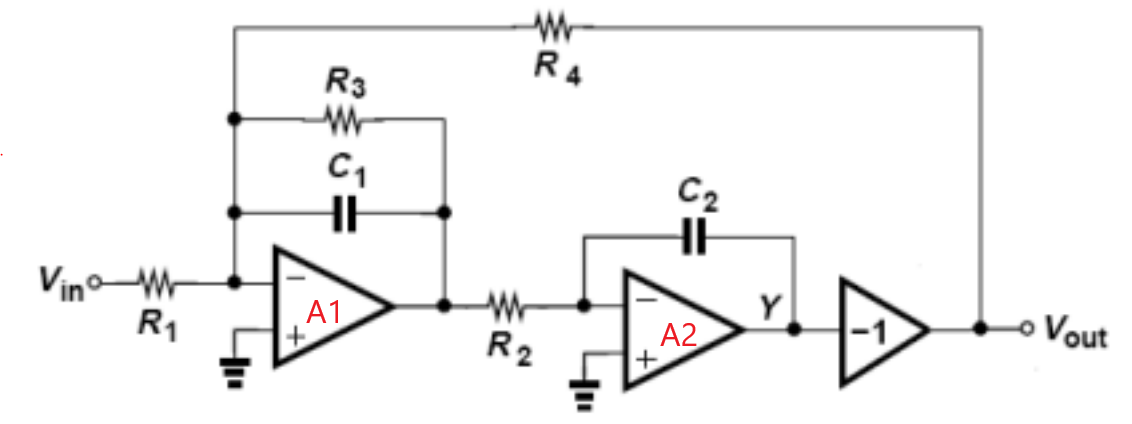
For the tow-thomas structure in the active filter, as shown in the figure below. There have been doubts about the phase margin of the amplifier!
捕获.PNG

We can design the amplifier's bandwidth to be relatively large, but at the same time how to consider the open-loop phase margin of the amplifier? We generally care about the bandwidth and phase margin of βA, but how is β calculated? After all, the filter in the figure above has three loops, namely the loop composed of amplifiers A1, R3, C1, and R1, the loop composed of amplifiers A2, C2, and R2, and the loop composed of amplifiers A1, A2, R4, and R1. So I am very puzzled, when designing amplifiers A1 and A2, how to calculate the β of these two amplifiers? What is the appropriate design of the phase margin of the open-loop amplifier?

Help me please, thx!!!
 

Hi,

For active filter design there is a rule of thumb for the OPAmp:.
Set the OPAmp's gain bandwidth product at least 10 times bigger than the closed loop filter's maximal gain bandwidth product.

Then set enough gain and phase margin for the OPAmps which guarantee they are unity gain stable, that is all.
In this case the OPAmp won't influence the characteristic of the active filter, even with parasitic and the whole system will be stable too.
This is a good way, but the brute force way of doing things. This way, you will be burning a lot of (unnecessary?) power simply amplifying signals that are not useful outside the band of interest. But, would be the last resort to fall back on. IMO, you can power-efficiently close the design if you put a little more effort in verification.

1. As for as the A1 is concerned, it sees two paths that close the loop around it 1) R3||C1 combination 2) through the A2 integrator feeding back. Just break the loop at the gate of A1 and do stability analysis and make sure you have good gain/phase margin.
2. Do the same for A2 too. For both A1 and A2, the stability should be checked when it is the actual filter network (ensuring unity gain stability is an overkill oftentimes).
3. Key thing to note in this process is this: The real amps should have enough gain at band edge (say ~15dB) so that you don't deviate a lot on the filter magnitude response. Lower gain will create higher droop at the band edge. The excess phase added by the non ideal integrators create peaking in the filter response at the band edge - which essentially attributes to the excess phase through the filter main loop, i.e phase margin of the main loop, which you can correct for the extra phase by re adjusting the filter caps and/or resistors that determine the poles of the filter.
 
  • Like
Reactions: FvM

This way, you will be burning a lot of (unnecessary?) power simply amplifying signals that are not useful outside the band of interest.
I think all active filter needs loop gain out of the desired band too, without loop gain there the stop band attenuation will be much lower. Other important thing the slewing to avoid, handling large signal behavior. So it is not unneccessary.

It is the brute force way absoluteley, but practical and you cannot do it too much better I think. In your point 3 with the extra 15dB gain you are telling almost the same, that ~10x bigger gain is needed. You saved 5dB, ok, that is fine, but if someone design TT biquad at the first time probably not the extra consumption caused by 5dB will be an issue, maybe, IDK.

You mention gain, but if the closed loop DC gain of the filter is not 0dB, higher, like 20dB, we don't know, then even 15dB extra gain is not enough. That is why I preferred to use gain bandwidth product.
 
  • Like
Reactions: FvM

Regarding required gain respectively GBW margin, it also depends on the designed biquad quality factor. The higher the quality factor, the higher the impact of a small amount of excessive integrator phase. The designed quality factor can be restored by reducing R3, but the filter characteristic becomes sensitive to PTV induced GBW variations. In so far, filter stability requirements set the minimum GBW demand.
 
Status
Not open for further replies.

Part and Inventory Search

Welcome to EDABoard.com

Sponsor

Back
Top