Continue to Site

Welcome to EDAboard.com

Welcome to our site! EDAboard.com is an international Electronics Discussion Forum focused on EDA software, circuits, schematics, books, theory, papers, asic, pld, 8051, DSP, Network, RF, Analog Design, PCB, Service Manuals... and a whole lot more! To participate you need to register. Registration is free. Click here to register now.

how to change negative gain to positive gain

demhaBay

Newbie
Joined
Dec 7, 2023
Messages
5
Helped
0
Reputation
0
Reaction score
0
Trophy points
1
Activity points
47
Good morning :
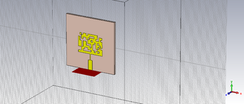
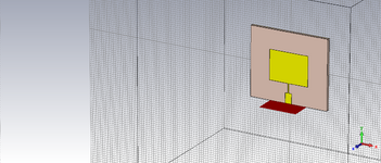
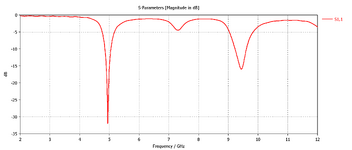
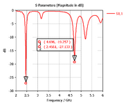
I'm working on the optimization of a rectangular patch antenna with matlab and Cst, and I find in the frequencies I find a negative gain up to -11.5 db, what is the method to follow to change the gain from negative to positive
 
Have you tried the forum search?

Negative gain results from loss in your antenna. Typically this is dielectric loss in the substrate. What is your substrate loss tangent, what is your design frequency?
 
Last edited:
hello Mr volker
I used an FR4 substrate with a permittivity of 4.3 and a tangent of 0.02.
The resonance frequency was initially set at 5 GHz, but after optimization, I obtained two peaks at 2.4 GHz and 3 GHz."
 
I don't think you can get positive power gain from a passive element.
Antenna "gain" is relative to some standard minimal antenna as far
as my limited RF knowledge says. Not an actual power out / power in
over unity.

Unless I missed the chapter about free lunches in all those books
I bought and didn't read.
 
@dick_freebird

Antenna gain is typically expressed in decibels (dB) and represents the increase in power or intensity in a particular direction when compared to an isotropic or spherical ideal radiator = 0 dBi

it's like focusing a light to a narrow beam which uses a lens to refract the beam with a magnification gain but with some loss due to the substrate.
The gain * half-power Beamwidth is constant is a lossless medium. The same is true to all antenna except avoiding the loss is critical as well as change in Dk the dielectric constant with higher frequencies which distorts the outcome.

This reminds me of my 1st Chinese Rolex copy watch (mid-80's) which was a gift and the lens over the date was the same dimension but wrong Dk of plastic was too high. An employee got it for me in a back lane in HK.

So low Dk, low loss substrates are preferred then patches can be tuned for gain by tuning the area of the patch.

His common problem is the dielectric choice is poor for 5 GHz which would show up in a spectral impedance plot.
 
@D.A.(Tony)Stewart
Thank you so much for your explanation, which makes understanding the problem easier. Of course, when I change the dielectric, I observe an increase in gain at the resonance peaks. My question is: with this FR4 substrate, is there a possibility to increase the gain by making certain modifications to the antenna geometry? This is crucial due to the cost of antenna fabrication
IDK, try some % geometry changes.

There are better FR4's so shop around Getek ML200? , FR408, Megtron6, etc. not much more $, also Tolerances on Dk are still 10% so change that too and use eff. Dk with Dk vs f curves.
Plexiglass?

Right now a short wire works better than your antenna with gain = -3 to+ 2 dB over this span.
 
Last edited:
My question is: with this FR4 substrate, is there a possibility to increase the gain by making certain modifications to the antenna geometry?
Yes, a simple 2.4 GHz patch antenna on FR4 gives +2.9dBi gain in my EM simulation, using tand=0.02 for substrate loss. Without substrate losses the gain would be around +6.7 dBi.

So even with lossy substrate, you should obtain a much better gain, using the most simple patch antenna geometry. It would really help if you show a picture of your antenna geometry.

Also, you should check what "gain" definition you have used in CST. See wikipedia: Realized gain differs from gain in that it is "reduced by its impedance mismatch factor." This mismatch induces losses above the dissipative losses described above; therefore, realized gain will always be less than gain.
 

- dielectric loss is proportional to the dielectric loss tangent and the square root of permittivity.
- conductor roughness matters too which adds path loss and alters thickness.
1702227085851.png


If all known losses do not add up, then your geometry is wrong. Do a sensitivity analysis for each dimension radius gap, thickness , DoE Taguchi method on Smith Chart.


So choose lower Dk and lower loss tangent < 0.01 but > 0.001 ($), try again
 
Last edited:
Hello everyone,

Thank you for your responses. I have images of the antennas. However, after optimizing the antenna, I encountered an issue with the gain becoming negative at 2.45 GHz. I am seeking advice on how to correct this anomaly.

Best regards,
 

Attachments

  • patch optim.png
    patch optim.png
    1 MB · Views: 79
  • patch.png
    patch.png
    894.6 KB · Views: 70
  • S11.png
    S11.png
    24 KB · Views: 61
  • 2.4g1.png
    2.4g1.png
    18.3 KB · Views: 61
It seems that you "optimized" your model for S11 only, and created a lossy resonator that doesn't radiate.
What is the goal of your opimization?
 
Interesting resonance for a random pixel antenna, but useful?.

I wonder what a snowflake antennae would look like.

I was always curious as a kid how geese could detect an airport flight path long before and fly around it until I saw the radar gain patterns of bird feathers in the library during Uni, then decades later seeing bird feather antenna designs on house tops for LMDS/MMDS over 20 yrs ago.
 
I agree with @volker@muehlhaus and @D.A.(Tony)Stewart.

@demhaBay

But I felt I needed to explain your important mistake.

You used the Lambda\4 (quarter-wave) impedance matching method. The quarter-wave impedance matching method matched only real impedance. It can't match the imaginary impedance. You should look impedance of your patch using an embedding waveguide port. Then you look at the end of Lambda\4 impedance. It must be conjugate impedance. And one step Lambda\4 impedance matching supports only their one frequency. You are arranging your frequency band using gaps in your patch. You can try two-step Lambda\4 impedance method. But you aren't still a match imaginary impedance. I suggest you use the stepped slot method for impedance matching. So, you can reduce your gap in the patch. Perhaps, (I think a high possibility) gaps in the patch reduce your realized gain.

I think parameter sweep is more useful than optimization algorithm. Maybe, you can reach better results using parameter sweep instead of optimization.

 
Thank you everyone for your clarification.
The goal of my optimization is to miniaturize a patch antenna, achieve dual-band or multiband functionality, and increase the bandwidth at the identified peaks using an optimization method. I am using quarter-wave line matching. A lingering question for me is whether this antenna will be useful. Is notch matching better than quarter-wave line matching or not? I will be using the parameters weep.
 

LaTeX Commands Quick-Menu:

Part and Inventory Search

Welcome to EDABoard.com

Sponsor

Back
Top