perado
Full Member level 2
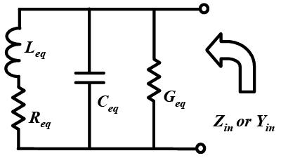
Y(s) that you drived at #8 ( Y(s)= gm1+ s Cgs1 + gm1 gm2 / (gds1+s Cgs2) ) is true and is like (5.7) equation of thesis but gm2 must place with gm1.
in this way the centeral frequency and Q can be drived as (5.12) and (5.13) that showed the relation of Q and central frequency with parameters,
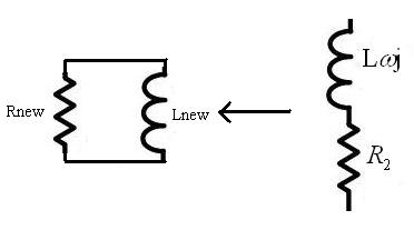
I simulated this circuit at 0.18um tsmc technology with ADS and saw the Q factor has direct relation with Cgs2 at low frequency and inverse relation with Cgs2 at higher frequency,
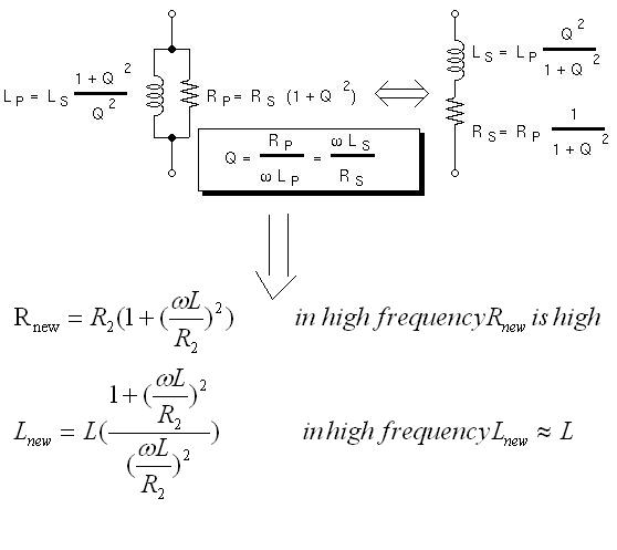
I read at this thesis (end line of page 93): "at high frequencies this approach is usually unsuccessful due to the excess phase error contributed by the interinsic device capacitances" , whats your idea about this? and if you think the Y(S) that drived with 2assumption is valid for all frequency range, then how I must describe the circuit simulation results?
in this way the centeral frequency and Q can be drived as (5.12) and (5.13) that showed the relation of Q and central frequency with parameters,
I simulated this circuit at 0.18um tsmc technology with ADS and saw the Q factor has direct relation with Cgs2 at low frequency and inverse relation with Cgs2 at higher frequency,
I read at this thesis (end line of page 93): "at high frequencies this approach is usually unsuccessful due to the excess phase error contributed by the interinsic device capacitances" , whats your idea about this? and if you think the Y(S) that drived with 2assumption is valid for all frequency range, then how I must describe the circuit simulation results?
")