asimov_18
Member level 2
- Joined
- Sep 25, 2006
- Messages
- 45
- Helped
- 2
- Reputation
- 4
- Reaction score
- 2
- Trophy points
- 1,288
- Location
- London---UK
- Activity points
- 1,816
Dear Member,
I am working on a research project that involves making a pulse generator
that generates square wave with peak to peak amplitude of 400V (+/- 200 V) at a frequency
of 1 MHz for driving capacitve loads of 50 pF. The design is possible as there are RF plasma generator
working in 2-3KW range with frequency of 13.56 MHz and I have disassembled one such RF generator.
I have come up with a design based on a datasheet/reference design by Microsemi DRF1400 (attached)
I have built it but it isn't working as expected!! And I am trying to figure out the problem hence
I am looking for inputs from members.
The design involves using a variac/auto transformer and a 1:1:1 turn ration isolation transformer.
The output of the secondary side of the transformer is rectified and followed by
bank of high voltage capacitor bank in order to generate the +200V and -200V
output(amplitude can be controlled by the varic connected to the primary side).
This part all working fine. Every thing working as expected!!
The second stage is made of of half bridge.
The high voltage is sent to a half bridge configuration made up of two N-channel
RF power MOSFETs DE150/DE275 from IXYS semiconductor. I don't think there are
equivalent P-channel devices hence the the bridge has to be made of N-channel MOSFETs.
Since both the high and the low side of the bridge are made up of a N-channel MOSFETs
one has to use separate isolated power supplies for generating the gate pulses as the source
of one MOSFET is not at the same potential as the source of the other(separated by potential difference of 400V)
and any gate control voltage is referenced with respect to source!! Also driving MOSFTEs at this high frequency
requires gate drivers as one has to quickly charge and discharge the gate capacitance
to turn on/off the MOSFETs. Interestingly DE150/275 has switching times of 5ns which is
very useful for high speed switching. As far as gate driving is concerned IXYS as single chip
solution IXRFD630 gate drivers which are matched for such application and are capable of
charging gates with surge currents up to 30 Amps!


The third critical aspect of the design is PCB layout as the tracks have to have minimum inductance
and one needs a lot of ground plane with generously placed decoupling capacitors(including tantalum capacitors)
for meeting the surge currents requirements. IXYS as a nice application note as an example for trying out
such designs. I have attached the application note for reference.
The gate control pulses are sent to the MOSFET drivers using Optical fiber cables (using Toshiba TOSLINK cables)
This gives a very high noise immunity to the gate drivers and ensure the pulses are not affected by electrical noise
as these CMOS gate driver chips are susceptible to electrical noise.
Also to ensure both the high and low side transistors are never switched on simultaneously I included another circuit
which ensure the two transistors can't be switched simultaneously. This circuit sends control signal to a Avago HCPL2201
very high speed optocoupler that can work up to 5 MHz.


The problem I am facing is as follows.
1) I can see the MOSFET gate driver generate very clean pulses when the MOSFETs are not connected to
the high voltage source. When connecting the high voltage source (+/-200V tried up to 50V initially)
the gate driver wave form get distorted.
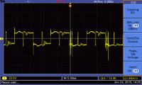
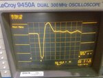
the second image shows the waveform getting distorted.
2) With the lower section of the bridge disconnected and no external load connected but only oscilloscope probe connected to the circuit, the upper
section of the bridge, the seems to be behaving strangely. The MOSFET switches on (pull-up) easily but when the pulse signals transition to low
state the output keeps lingering close to Vcc this happens even at low frequency say 100 KHz, The actual switching off can only be seen for very
low frequency signal say 100 Hz other wise for any frequency higher than that the output stays at Vcc.
My assumption was because when the MOSFET is turned on the charge carriers are pulled to create the channel region/inversion layer there needs to be be
some mechanism to remove these charge carriers in order for the channel to disappear and the MOSFET to switch off, this could either happen
over time if the switching frequency is very slow or if there is an external load/dummy resistor connected to the output which would drain this charge.
I was surprised this reasoning seems to be actually true as I connected a 100W incandescent lamp at the out output as load and get the MOSFET to switch up of 10KHz
with reasonable fall times. I guessed with the lower section of the bridge active the pull down would also become fast as there was an active
element(the lower MOSFET) pulling the output low dissipating the charge accumulated making up the channel region.
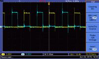
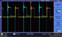
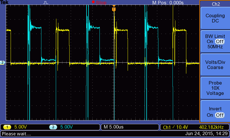
3) With the complete bridge circuit where both lower and higher side of the bridge are connected I am still not seeing a square wave output.
I see a very strange signal output. Image attached. Infact there is thru conduction taking place across the bridge. This happens despite there
being sufficient delay between the pulses being used to trigger the lower and upper MOSFETs making up the bridge. This is further confirmed
as I have safety fuses connected to the supply rail which blow up confirming a thru conduction! In fact I managed to destroy one set of MOSFETs
even before the usual glass cartridge fuse could react!!
Could any one give me some inputs/ suggestions where to look for the problem?
Any help would be highly appreciated.
Regards
Asimov
I am working on a research project that involves making a pulse generator
that generates square wave with peak to peak amplitude of 400V (+/- 200 V) at a frequency
of 1 MHz for driving capacitve loads of 50 pF. The design is possible as there are RF plasma generator
working in 2-3KW range with frequency of 13.56 MHz and I have disassembled one such RF generator.
I have come up with a design based on a datasheet/reference design by Microsemi DRF1400 (attached)
I have built it but it isn't working as expected!! And I am trying to figure out the problem hence
I am looking for inputs from members.
The design involves using a variac/auto transformer and a 1:1:1 turn ration isolation transformer.
The output of the secondary side of the transformer is rectified and followed by
bank of high voltage capacitor bank in order to generate the +200V and -200V
output(amplitude can be controlled by the varic connected to the primary side).
This part all working fine. Every thing working as expected!!
The second stage is made of of half bridge.
The high voltage is sent to a half bridge configuration made up of two N-channel
RF power MOSFETs DE150/DE275 from IXYS semiconductor. I don't think there are
equivalent P-channel devices hence the the bridge has to be made of N-channel MOSFETs.
Since both the high and the low side of the bridge are made up of a N-channel MOSFETs
one has to use separate isolated power supplies for generating the gate pulses as the source
of one MOSFET is not at the same potential as the source of the other(separated by potential difference of 400V)
and any gate control voltage is referenced with respect to source!! Also driving MOSFTEs at this high frequency
requires gate drivers as one has to quickly charge and discharge the gate capacitance
to turn on/off the MOSFETs. Interestingly DE150/275 has switching times of 5ns which is
very useful for high speed switching. As far as gate driving is concerned IXYS as single chip
solution IXRFD630 gate drivers which are matched for such application and are capable of
charging gates with surge currents up to 30 Amps!
The third critical aspect of the design is PCB layout as the tracks have to have minimum inductance
and one needs a lot of ground plane with generously placed decoupling capacitors(including tantalum capacitors)
for meeting the surge currents requirements. IXYS as a nice application note as an example for trying out
such designs. I have attached the application note for reference.
The gate control pulses are sent to the MOSFET drivers using Optical fiber cables (using Toshiba TOSLINK cables)
This gives a very high noise immunity to the gate drivers and ensure the pulses are not affected by electrical noise
as these CMOS gate driver chips are susceptible to electrical noise.
Also to ensure both the high and low side transistors are never switched on simultaneously I included another circuit
which ensure the two transistors can't be switched simultaneously. This circuit sends control signal to a Avago HCPL2201
very high speed optocoupler that can work up to 5 MHz.
The problem I am facing is as follows.
1) I can see the MOSFET gate driver generate very clean pulses when the MOSFETs are not connected to
the high voltage source. When connecting the high voltage source (+/-200V tried up to 50V initially)
the gate driver wave form get distorted.

the second image shows the waveform getting distorted.

2) With the lower section of the bridge disconnected and no external load connected but only oscilloscope probe connected to the circuit, the upper
section of the bridge, the seems to be behaving strangely. The MOSFET switches on (pull-up) easily but when the pulse signals transition to low
state the output keeps lingering close to Vcc this happens even at low frequency say 100 KHz, The actual switching off can only be seen for very
low frequency signal say 100 Hz other wise for any frequency higher than that the output stays at Vcc.
My assumption was because when the MOSFET is turned on the charge carriers are pulled to create the channel region/inversion layer there needs to be be
some mechanism to remove these charge carriers in order for the channel to disappear and the MOSFET to switch off, this could either happen
over time if the switching frequency is very slow or if there is an external load/dummy resistor connected to the output which would drain this charge.
I was surprised this reasoning seems to be actually true as I connected a 100W incandescent lamp at the out output as load and get the MOSFET to switch up of 10KHz
with reasonable fall times. I guessed with the lower section of the bridge active the pull down would also become fast as there was an active
element(the lower MOSFET) pulling the output low dissipating the charge accumulated making up the channel region.
3) With the complete bridge circuit where both lower and higher side of the bridge are connected I am still not seeing a square wave output.
I see a very strange signal output. Image attached. Infact there is thru conduction taking place across the bridge. This happens despite there
being sufficient delay between the pulses being used to trigger the lower and upper MOSFETs making up the bridge. This is further confirmed
as I have safety fuses connected to the supply rail which blow up confirming a thru conduction! In fact I managed to destroy one set of MOSFETs
even before the usual glass cartridge fuse could react!!
Could any one give me some inputs/ suggestions where to look for the problem?
Any help would be highly appreciated.
Regards
Asimov
")