Geekyguy
Newbie level 3
Hi guys,
How are you all? I am trying to build to a PLL circuits. As part of the circuit, I will need an offset adder, integrator, rectifier, and another stage of offset adder.
I havent done circuits for very long time. So please bear with me if Im crapping.
Appreciate your help.
I have designed the first stage offset adder and integrator.
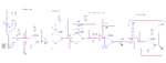
Please see attached diagrams. Schematic 1 is the circuit for offset adder which basically a summing amplifier, and then the second stage op-amp is the integrator.
The AC source with 1 Vac, is passed through the R3 and R1, R3 will later be a variable resistor when I transfer this to PCB.
From the diagram, I dont understand how the 5V added by V2 becomes 2.5V at the output of U1 (first Op-amp). I tried calculating it out, but could not get the exact point. Please advice.
Then, at the second stage. If you see the frequency response diagram. The 3dB is approximately at 200 kHz. But by using 1/2\[\prod\]RC formula, R=R3 and C=C1, which are 1 kohm and 50 pF, respectively, the cutoff should be approximately 3.1 MHz. So I dont really get it. Please advice if Im in the right direction, or the equivalent circuit calculation is wrong.
Please point where Im going wrong. I have also attached the time domain graph.
Thank you so much.


How are you all? I am trying to build to a PLL circuits. As part of the circuit, I will need an offset adder, integrator, rectifier, and another stage of offset adder.
I havent done circuits for very long time. So please bear with me if Im crapping.
Appreciate your help.
I have designed the first stage offset adder and integrator.
Please see attached diagrams. Schematic 1 is the circuit for offset adder which basically a summing amplifier, and then the second stage op-amp is the integrator.
The AC source with 1 Vac, is passed through the R3 and R1, R3 will later be a variable resistor when I transfer this to PCB.
From the diagram, I dont understand how the 5V added by V2 becomes 2.5V at the output of U1 (first Op-amp). I tried calculating it out, but could not get the exact point. Please advice.
Then, at the second stage. If you see the frequency response diagram. The 3dB is approximately at 200 kHz. But by using 1/2\[\prod\]RC formula, R=R3 and C=C1, which are 1 kohm and 50 pF, respectively, the cutoff should be approximately 3.1 MHz. So I dont really get it. Please advice if Im in the right direction, or the equivalent circuit calculation is wrong.
Please point where Im going wrong. I have also attached the time domain graph.
Thank you so much.