Continue to Site

Welcome to EDAboard.com

Welcome to our site! EDAboard.com is an international Electronics Discussion Forum focused on EDA software, circuits, schematics, books, theory, papers, asic, pld, 8051, DSP, Network, RF, Analog Design, PCB, Service Manuals... and a whole lot more! To participate you need to register. Registration is free. Click here to register now.

Help with a diode-connected NMOS

Status
Not open for further replies.

desperatejobseeker

Newbie level 5
Joined
Mar 21, 2012
Messages
10
Helped
1
Reputation
2
Reaction score
1
Trophy points
1,283
Location
shanghai, china
Activity points
1,369
Hi all,

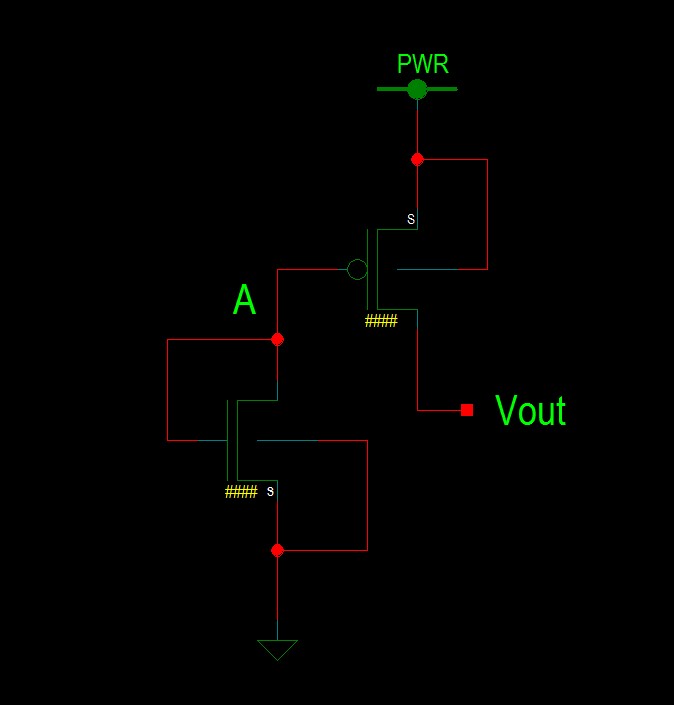
An NMOS is dioded-connected, that has its Gate/Drain tied to another PMOS gate and both its body and souce are tied to gnd. I saw many schematics using this kind of structure, I wonder how it could work? Although for the NMOS Vds>Vgs-Vth, from my perspective, there is no voltage bias at Gate/Drain, cuz they r only tied together to the gate of another PMOS. How could it possible work?

Thanks in advance!
 

what is the voltage at node A?

- - - Updated - - -

what is the voltage at node A?
 

Attachments

  • 2012-06-12 13 28 04.jpg
    2012-06-12 13 28 04.jpg
    21.6 KB · Views: 72

what is the voltage at node A?

- - - Updated - - -

what is the voltage at node A?

Unless I'm seriously off - A should be around Vth of the NMOS.
The way the NMOS is connected - gate to drain - means that it's either cutoff or in saturation. Since it's connected to the gate of the PMOS, a capacitor, the NMOS will conduct current until the PMOS gate voltage reaches Vth (either charging or discharging it) at which point the NMOS will be cutoff.

If Vth_nmos-Vpwr<Vth_pmos then the PMOS will always conduct current. Whether the PMOS is in triode or saturation region depends on how much voltage falls across the load.
 
Last edited:

So the diode-connected NMOS acts like a resistor with a value of 1/gm, and it always works in the saturation region, which means Vgs of the NMOS should at least bigger than Vth, the voltage at A should be equal or larger than Vth. But I am still curious that since only a PMOS gate is connected to the node A, no one else can provide power to this node, where did such voltage come from?

- - - Updated - - -

Imagine we replace a resistor of the diode-connected NMOS, one end of resistor is grounded and the other end is connected to the gate of PMOS. In this situation, is the voltage at node A should be zero?
 

I don't know what schematics you are looking at, but it's pretty much a useless structure.
Node A is a high impedance node, aka a floating input.

On power up, the voltage would depend on the capacitive divider of any parasitic caps on that node.
Run a switching signal over this line and all sorts noise would be coupled onto it.
It would be subject to leakage currents.
In other words, the voltage of that node can be anything, and the true voltage is unlikely to be able to be simulated.

If this is used in a practical circuit, the designer ought to be sent back to school.
 

I don't really know if this structure is useless or not, but what I am 100% percent sure is this structure has been put into practice and developed a large scale production.
 

I don't know what schematics you are looking at, but it's pretty much a useless structure.
Node A is a high impedance node, aka a floating input.

On power up, the voltage would depend on the capacitive divider of any parasitic caps on that node.
Run a switching signal over this line and all sorts noise would be coupled onto it.
It would be subject to leakage currents.
In other words, the voltage of that node can be anything, and the true voltage is unlikely to be able to be simulated.

If this is used in a practical circuit, the designer ought to be sent back to school.

If the Voltage at Node A is higher than Vth, the NMOS will be in saturation and discharge the node A until Va<Vth, so Va will never higher than Vth of the NMOS.
 

If the Voltage at Node A is higher than Vth, the NMOS will be in saturation and discharge the node A until Va<Vth, so Va will never higher than Vth of the NMOS.
It's pointless harping on when Node A is higher than Vth.

It will only be so if some parasitic cap stores some charges to generate a greater than Vth voltage.
The question comes with how these charges actually accumulate on Node A? Capacitive coupling? Leakage currents? Some nearby wire? Charges coupled from the PMOS source/drains? All these are not reliable drivers for Node A.

Even when it occurs, the NMOS will conduct these charges away in a split second, and then what?
 

At steady state, the voltage on node A will be zero. Even if some charge is injected into node A (through capacitive coupling or etc.), the NMOS will conduct it down. Once Va < Vth, the NMOS goes into subthreshold conduction -- i.e., it's still conducting. It continues to conduct until node A is completely discharged. Therefore, the PMOS will be fully-on.

The circuit as drawn is generally useless.
 
Status
Not open for further replies.

Similar threads

Part and Inventory Search

Welcome to EDABoard.com

Sponsor

Back
Top