Quantum.Dot
Newbie level 6
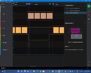
Having Issues With Full-Bridge Signals [ Code MPLAB-X XC8 ]
This is my code.
This is my code.
Code:
/*
 * File:   main.c
 * Author: Quantum.Dot
 *
 * Created on 2 April, 2022, 11:48 PM
 */

#define _XTAL_FREQ 16000000UL


// PIC18F45K22 Configuration Bit Settings

// 'C' source line config statements

// CONFIG1H
#pragma config FOSC = INTIO67   // Oscillator Selection bits (Internal oscillator block)
#pragma config PLLCFG = ON     // 4X PLL Enable (Oscillator used directly)
#pragma config PRICLKEN = ON    // Primary clock enable bit (Primary clock is always enabled)
#pragma config FCMEN = ON       // Fail-Safe Clock Monitor Enable bit (Fail-Safe Clock Monitor enabled)
#pragma config IESO = ON        // Internal/External Oscillator Switchover bit (Oscillator Switchover mode enabled)

// CONFIG2L
#pragma config PWRTEN = ON      // Power-up Timer Enable bit (Power up timer enabled)
#pragma config BOREN = ON       // Brown-out Reset Enable bits (Brown-out Reset enabled and controlled by software (SBOREN is enabled))
#pragma config BORV = 285       // Brown Out Reset Voltage bits (VBOR set to 2.85 V nominal)

// CONFIG2H
#pragma config WDTEN = ON      // Watchdog Timer Enable bits (Watch dog timer is always disabled. SWDTEN has no effect.)
#pragma config WDTPS = 1024     // Watchdog Timer Postscale Select bits (1:1024)

// CONFIG3H
#pragma config CCP2MX = PORTC1  // CCP2 MUX bit (CCP2 input/output is multiplexed with RC1)
#pragma config PBADEN = OFF     // PORTB A/D Enable bit (PORTB<5:0> pins are configured as digital I/O on Reset)
#pragma config CCP3MX = PORTB5  // P3A/CCP3 Mux bit (P3A/CCP3 input/output is multiplexed with RB5)
#pragma config HFOFST = ON      // HFINTOSC Fast Start-up (HFINTOSC output and ready status are not delayed by the oscillator stable status)
#pragma config T3CMX = PORTC0   // Timer3 Clock input mux bit (T3CKI is on RC0)
#pragma config P2BMX = PORTD2   // ECCP2 B output mux bit (P2B is on RD2)
#pragma config MCLRE = INTMCLR  // MCLR Pin Enable bit (RE3 input pin enabled; MCLR disabled)

// CONFIG4L
#pragma config STVREN = ON      // Stack Full/Underflow Reset Enable bit (Stack full/underflow will cause Reset)
#pragma config LVP = OFF        // Single-Supply ICSP Enable bit (Single-Supply ICSP disabled)
#pragma config XINST = OFF      // Extended Instruction Set Enable bit (Instruction set extension and Indexed Addressing mode disabled (Legacy mode))

// CONFIG5L
#pragma config CP0 = OFF        // Code Protection Block 0 (Block 0 (000800-001FFFh) not code-protected)
#pragma config CP1 = OFF        // Code Protection Block 1 (Block 1 (002000-003FFFh) not code-protected)
#pragma config CP2 = OFF        // Code Protection Block 2 (Block 2 (004000-005FFFh) not code-protected)
#pragma config CP3 = OFF        // Code Protection Block 3 (Block 3 (006000-007FFFh) not code-protected)

// CONFIG5H
#pragma config CPB = OFF        // Boot Block Code Protection bit (Boot block (000000-0007FFh) not code-protected)
#pragma config CPD = OFF        // Data EEPROM Code Protection bit (Data EEPROM not code-protected)

// CONFIG6L
#pragma config WRT0 = OFF       // Write Protection Block 0 (Block 0 (000800-001FFFh) not write-protected)
#pragma config WRT1 = OFF       // Write Protection Block 1 (Block 1 (002000-003FFFh) not write-protected)
#pragma config WRT2 = OFF       // Write Protection Block 2 (Block 2 (004000-005FFFh) not write-protected)
#pragma config WRT3 = OFF       // Write Protection Block 3 (Block 3 (006000-007FFFh) not write-protected)

// CONFIG6H
#pragma config WRTC = OFF       // Configuration Register Write Protection bit (Configuration registers (300000-3000FFh) not write-protected)
#pragma config WRTB = OFF       // Boot Block Write Protection bit (Boot Block (000000-0007FFh) not write-protected)
#pragma config WRTD = OFF       // Data EEPROM Write Protection bit (Data EEPROM not write-protected)

// CONFIG7L
#pragma config EBTR0 = OFF      // Table Read Protection Block 0 (Block 0 (000800-001FFFh) not protected from table reads executed in other blocks)
#pragma config EBTR1 = OFF      // Table Read Protection Block 1 (Block 1 (002000-003FFFh) not protected from table reads executed in other blocks)
#pragma config EBTR2 = OFF      // Table Read Protection Block 2 (Block 2 (004000-005FFFh) not protected from table reads executed in other blocks)
#pragma config EBTR3 = OFF      // Table Read Protection Block 3 (Block 3 (006000-007FFFh) not protected from table reads executed in other blocks)

// CONFIG7H
#pragma config EBTRB = OFF      // Boot Block Table Read Protection bit (Boot Block (000000-0007FFh) not protected from table reads executed in other blocks)

// #pragma config statements should precede project file includes.
// Use project enums instead of #define for ON and OFF.

#include <xc.h>

#define scrGateTriggerPin LATD0
#define outputFullBridgeGateTriggerPin LATD1
#define LedPin  LATD2
#define zcdMimicPin LATB1

unsigned int state = 0;
unsigned int zcdCount = 0;
unsigned int timer2InterruptCount = 0;

unsigned int voltage = 0;
unsigned int frequency = 0;
unsigned int loadCurrent = 0;

unsigned sinewaveLutIndex = 0;

unsigned int sinewaveLUT[32] = {0,10,39,86,149,226,314,410,509,608,704,792,869,932,979,1008,1018,1008,979,932,869,792,704,608,
509,410,314,226,149,86,39,10};

/*
unsigned int sinewaveLUT[32] = {509,608,704,792,869,932,979,1008,1018,1008,979,932,869,792,704,608,
509,410,314,226,149,86,39,10,0,10,39,86,149,226,314,410};
*/

//Timer1
//Prescaler 1:4; TMR1 Preload = 25536; Actual Interrupt Time : 10 ms

//Place/Copy this part in declaration section
void InitTimer1() {
    T1CON = 0x21;
    TMR1IF = 0;
    TMR1H = 0x63;
    TMR1L = 0xC0;
    TMR1IE = 1;
}

//Timer2
//Prescaler 1:1; Postscaler 1:4; TMR2 Preload = 249; Actual Interrupt Time : 62.5 us
void InitTimer2(){
    T2CON = 0x1C;
    TMR2IE = 1;
    PR2 = 249;
    TMR2ON = 0;
}

void __interrupt () my_isr_routine (void) {
    if((TMR2IE) && (TMR2IF)) {
        TMR2IF = 0;
        scrGateTriggerPin = 0;
        //Enter your code here
        if(timer2InterruptCount++ == 5) {
            timer2InterruptCount = 0;
            if(++sinewaveLutIndex == 32) {
               sinewaveLutIndex = 0;
               P1M1 = ~P1M1;
            }
        }

        CCPR1L = (unsigned char)sinewaveLUT[sinewaveLutIndex];
        DC1B1 = ((sinewaveLUT[sinewaveLutIndex] >> 9) & 0x01);
        DC1B0 = ((sinewaveLUT[sinewaveLutIndex] >> 8) & 0x01);
    }

    if((TMR1IE) && (TMR1IF)) {
        TMR1IF = 0;
        TMR1H = 0x63;
        TMR1L = 0xC0;
        //Enter your code here
        zcdMimicPin = ~zcdMimicPin;
    }

    if((INT0IE) && (INT0IF)) {
        INT0IF = 0;
        INTEDG0 = ~INTEDG0;
        scrGateTriggerPin = 1;
        //Enter your code here
        if((zcdCount++ % 50) == 0)LedPin = ~LedPin;

        __asm ("nop");
        __asm ("nop");
        __asm ("nop");
        __asm ("nop");
        __asm ("nop");
        __asm ("nop");
        __asm ("nop");
        __asm ("nop");
        __asm ("nop");
        __asm ("nop");

        __asm ("nop");
        __asm ("nop");
        __asm ("nop");
        __asm ("nop");
        __asm ("nop");
        __asm ("nop");
        __asm ("nop");
        __asm ("nop");
        __asm ("nop");
        __asm ("nop");

        __asm ("nop");
        __asm ("nop");
        __asm ("nop");
        __asm ("nop");
        __asm ("nop");
        __asm ("nop");
        __asm ("nop");
        __asm ("nop");
        __asm ("nop");
        __asm ("nop");

        __asm ("nop");
        __asm ("nop");
        __asm ("nop");
        __asm ("nop");
        __asm ("nop");
        __asm ("nop");
        __asm ("nop");
        __asm ("nop");
        __asm ("nop");
        __asm ("nop");

        __asm ("nop");
        __asm ("nop");
        __asm ("nop");
        __asm ("nop");
        __asm ("nop");
        __asm ("nop");
        __asm ("nop");
        __asm ("nop");
        __asm ("nop");
        __asm ("nop");

        __asm ("nop");
        __asm ("nop");
        __asm ("nop");
        __asm ("nop");
        __asm ("nop");
        __asm ("nop");
        __asm ("nop");
        __asm ("nop");
        __asm ("nop");
        __asm ("nop");

        __asm ("nop");
        __asm ("nop");
        __asm ("nop");
        __asm ("nop");
        __asm ("nop");
        __asm ("nop");
        __asm ("nop");
        __asm ("nop");
        __asm ("nop");
        __asm ("nop");

        __asm ("nop");
        __asm ("nop");
        __asm ("nop");
        __asm ("nop");
        __asm ("nop");
        __asm ("nop");
        __asm ("nop");
        __asm ("nop");
        __asm ("nop");
        __asm ("nop");

        __asm ("nop");
        __asm ("nop");
        __asm ("nop");
        __asm ("nop");
        __asm ("nop");
        __asm ("nop");
        __asm ("nop");
        __asm ("nop");
        __asm ("nop");
        __asm ("nop");

        __asm ("nop");
        __asm ("nop");
        __asm ("nop");
        __asm ("nop");
        __asm ("nop");
        __asm ("nop");
        __asm ("nop");
        __asm ("nop");
        __asm ("nop");
        __asm ("nop");

        __asm ("nop");
        __asm ("nop");
        __asm ("nop");
        __asm ("nop");
        __asm ("nop");
        __asm ("nop");
        __asm ("nop");
        __asm ("nop");
        __asm ("nop");
        __asm ("nop");

        __asm ("nop");
        __asm ("nop");
        __asm ("nop");
        __asm ("nop");
        __asm ("nop");
        __asm ("nop");
        __asm ("nop");
        __asm ("nop");
        __asm ("nop");
        __asm ("nop");

        __asm ("nop");
        __asm ("nop");
        __asm ("nop");
        __asm ("nop");
        __asm ("nop");
        __asm ("nop");
        __asm ("nop");
        __asm ("nop");
        __asm ("nop");
        __asm ("nop");

        __asm ("nop");
        __asm ("nop");
        __asm ("nop");
        __asm ("nop");
        __asm ("nop");
        __asm ("nop");
        __asm ("nop");
        __asm ("nop");
        __asm ("nop");
        __asm ("nop");

        __asm ("nop");
        __asm ("nop");
        __asm ("nop");
        __asm ("nop");
        __asm ("nop");
        __asm ("nop");
        __asm ("nop");
        __asm ("nop");
        __asm ("nop");
        __asm ("nop");

        __asm ("nop");
        __asm ("nop");
        __asm ("nop");
        __asm ("nop");
        __asm ("nop");
        __asm ("nop");
        __asm ("nop");
        __asm ("nop");
        __asm ("nop");
        __asm ("nop");
        //...

        scrGateTriggerPin = 0;
        if(!TMR2ON)TMR2ON = 1;
    }
}

void main(void) {
    OSCCON = 0b01110000;
    OSCCON2 = 0b00000111;
    OSCTUNE = 0b01000000;

    CM1CON0 = 0b00000000;
    CM2CON0 = 0b00000000;

    SLRCON = 0b00000000;

    ADCON1 = 0b00000000;
    ADCON2 = 0b10110101;

    ANSELA = 0b00000000;
    ANSELB = 0b00000000;
    ANSELC = 0b00000000;
    ANSELD = 0b00000000;
    ANSELE = 0b00000000;

    TRISA = 0b00000000;
    TRISB = 0b00000001;
    TRISC = 0b00000000;
    TRISD = 0b11111111;
    TRISE = 0b00000000;

    PORTA = 0b00000000;
    PORTB = 0b00000000;
    PORTC = 0b00000000;
    PORTD = 0b00000000;
    PORTE = 0b00000000;

    LATA = 0b00000000;
    LATB = 0b00000000;
    LATC = 0b00000000;
    LATD = 0b00000000;
    LATE = 0b00000000;

    P1M0 = 1;
    P1M1 = 0;

    INTEDG0 = 1;
    INT0IF = 0;
    INT0IE = 1;

    CCP1M0 = 1;
    CCP1M1 = 0;
    CCP1M2 = 1;
    CCP1M3 = 1;

    CCPR1L = 0;
    DC1B0 = 0;
    DC1B1 = 0;

    InitTimer2();
    TRISD = 0b00000000;

    InitTimer1();

    PEIE = 1;
    GIE = 1;

    while(1) {
        __asm("clrwdt");
    }

    return;
}
Attachments
Last edited by a moderator: