Continue to Site

Welcome to EDAboard.com

Welcome to our site! EDAboard.com is an international Electronics Discussion Forum focused on EDA software, circuits, schematics, books, theory, papers, asic, pld, 8051, DSP, Network, RF, Analog Design, PCB, Service Manuals... and a whole lot more! To participate you need to register. Registration is free. Click here to register now.

Gnd connection for chip inductor

Status
Not open for further replies.

Lathas

Advanced Member level 4
Joined
Oct 16, 2012
Messages
118
Helped
1
Reputation
2
Reaction score
1
Trophy points
1,298
Activity points
2,044
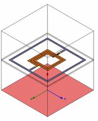
Looking at the example given by HFSS manual, I can see a ring around the inductor acting as a gnd reference for the port, but it is not connected to the actual gnd underneath(below the silicon), so how does it work? Should the ring be connected to the gnd below in the actual implementation?


Should the ring be connected to the gnd below in the actual implementation?

No. Ground is whatever you use/connect for ground return, and this is always on the top side of the chip. The bottom side is floating.
 
  • Like
Reactions: Lathas

    Lathas

    Points: 2
    Helpful Answer Positive Rating
Thanks! Should this be a ring/closed loop itself? How do you choose the width of the gnd conductor or distance of gnd ring from the inductor?
 

Thanks! Should this be a ring/closed loop itself? How do you choose the width of the gnd conductor or distance of gnd ring from the inductor?

The ring represents a closed metal boundary in the chip, where return current can flow in real hardware. So that gives you the dimensions: same as hardware. It is important to understand that this ring forms a shorted secondary loop around the inductors, so it has some negative effect. Unfortunately in HFSS you can't model inductors without such a return path, and on chip (hardware) you also need some return path.

The trick is to have "enough" distance between the inductor and the ground frame, and "enough" depends on multiple factors like number of turns etc. Note that larger distance from inductor to ground ring also means longer feed lines, which are included in results and degrade the Q factor.

Sometimes designers use a slotted frame (not closed loop) when inductors have both terminals on one side.

This inductor designs is somewhat tricky, and it can take time to get a feeling for "good" methodology.
 
  • Like
Reactions: Lathas

    Lathas

    Points: 2
    Helpful Answer Positive Rating
Can I take Rdc = re(1/Yin) at 0hz in this design?
 
Last edited:

Can I take Rdc = re(1/Yin) at 0hz in this design?

If you want to measure the resistance of the full path (including return path in ground frame), then yes.
Obviously the width of your ground frame matters in this case.
 
  • Like
Reactions: Lathas

    Lathas

    Points: 2
    Helpful Answer Positive Rating
Status
Not open for further replies.

Similar threads

Part and Inventory Search

Welcome to EDABoard.com

Sponsor

Back
Top