Welcome to our site! EDAboard.com is an international Electronics Discussion Forum focused on EDA software, circuits, schematics, books, theory, papers, asic, pld, 8051, DSP, Network, RF, Analog Design, PCB, Service Manuals... and a whole lot more! To participate you need to register. Registration is free. Click here to register now.
The idea of getting rid of antenna errors is to save gate from static charges that got itself on long metal connected somehow to gate. It doesn't mean you will get antenna violation on top of metal 1, you might get on any metal. Check your error report as to know on which metal you got the error. Then from error report you can calculate maximum how much length of that metal is allowed to be connected to gate. So that particular metal should extend from the gate connection upto that calculated distance. Then place jumper on that metal.
Or else if you can't calculate the length, you simply allow very less metal (on which antenna error is coming) to be connected to gate, and then place a jumper. Will get the job for you.
No matter how many metal layer jumps you're using, if the accumulated metal area gets too large in relation to the gate area, you'll get an antenna violation. The clue is to have a connection to a junction (to GND or VDD) somewhere in the metal path, close enough to the gate: either any output, or a protection diode of an input pad. If that isn't available, use an extra - normally reverse-biased - diode near the concerned gate.
Generally for this GNAC diode is used. It works in reverse bias. Probably it's a Zener Diode, but not sure. Anyways a diode in reverse bias adds leakage. So adding GNAC should be the last thing to do. But even before that you should ask the schematic designer.
eriki, am I right? Please reply.
... Probably it's a Zener Diode, but not sure. Anyways a diode in reverse bias adds leakage. So adding GNAC should be the last thing to do. But even before that you should ask the schematic designer.
eriki, am I right? Please reply.
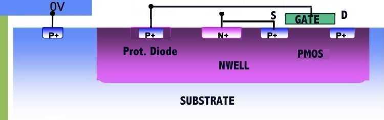
No Zener, a standard diode will do the job, see e.g. this example for the protection of a pMOS gate:
Of course it will add reverse leakage current, but one needs a reverse-bias junction in any case, because there's no other chance to protect a gate against antenna violation. And it should be near enough, before the metal connection area exceeds the tolerable value (in relation to the gate area).
BTW: A real designer will foresee the necessity of such a diode (if there exists no near junction like an output connection) and will define such a protection diode in schematics, including a notice to layout it near the gate.
A jumper only protects against antenna charging from layers
below it. If (say) you broke and jumpered Met1 with a Met2
strap, that's fine for Met1 (assuming the jumper is close to
the gate ox to be protected) but remote Met2 attached to
the gate, through that Met1 trace, is not stood off by the
pre-jumper gap because that gap is not there after Met2 dep.
The idea of getting rid of antenna errors is to save gate from static charges that got itself on long metal connected somehow to gate. It doesn't mean you will get antenna violation on top of metal 1, you might get on any metal. Check your error report as to know on which metal you got the error. Then from error report you can calculate maximum how much length of that metal is allowed to be connected to gate. So that particular metal should extend from the gate connection upto that calculated distance. Then place jumper on that metal.
Or else if you can't calculate the length, you simply allow very less metal (on which antenna error is coming) to be connected to gate, and then place a jumper. Will get the job for you.
u mean by placing, gate->m1->m2->m1 (where m2 is a jumper for m1)is fine but, if m2 is long then it gives antenna violation???
which means m3 jumper is to be used for m2!!!
u mean by placing, gate->m1->m2->m1 (where m2 is a jumper for m1)is fine but, if m2 is long then it gives antenna violation???
which means m3 jumper is to be used for m2!!!
Thats correct .
This is what suggested by "VLSI_Learner " . First check which metal is giving antenna and add jumper of next higher metal as near to gate as possible . Hopefully this should resolve .
This site uses cookies to help personalise content, tailor your experience and to keep you logged in if you register.
By continuing to use this site, you are consenting to our use of cookies.