Continue to Site

Welcome to EDAboard.com

Welcome to our site! EDAboard.com is an international Electronics Discussion Forum focused on EDA software, circuits, schematics, books, theory, papers, asic, pld, 8051, DSP, Network, RF, Analog Design, PCB, Service Manuals... and a whole lot more! To participate you need to register. Registration is free. Click here to register now.

eye diagram getting worse reasons of buffer

Status
Not open for further replies.

yefj

Advanced Member level 4
Joined
Sep 12, 2019
Messages
1,239
Helped
1
Reputation
2
Reaction score
3
Trophy points
38
Activity points
7,463
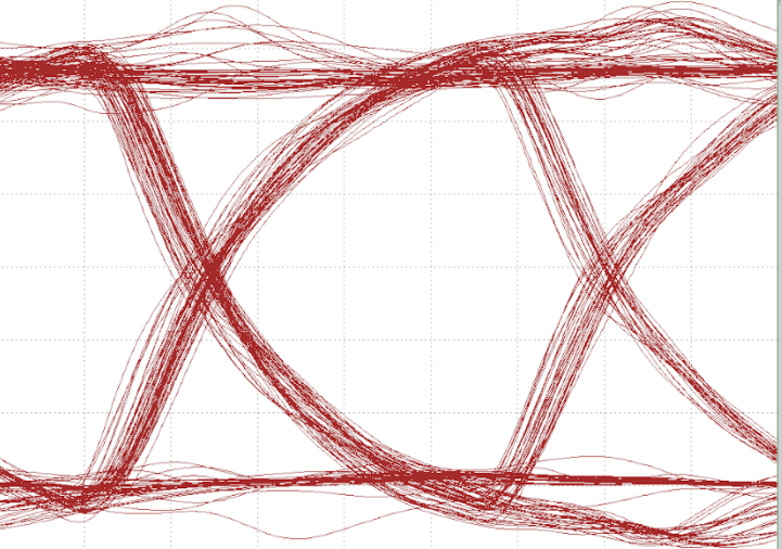
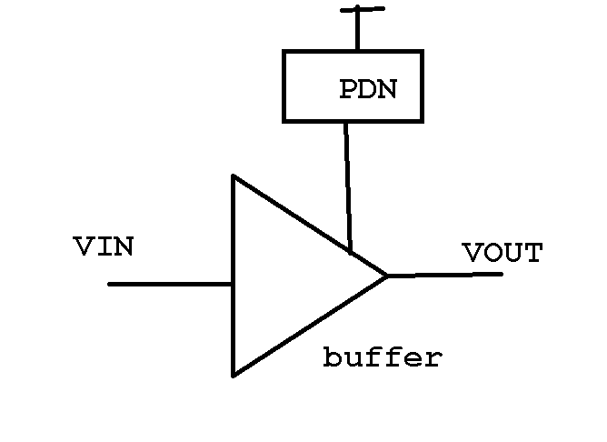
Hello,from the buffer system bellow i get the eye diagram,the problem with this eye diagram is the walls and by their thickness we see the quality of the signal.
What cause the top and bottom wall to get thicker?
I know that if we have higher PDN resistance then Vout capacitor will be charged to less voltage because of voltage divider.

What about the walls on the left and right , the vertical ones
What cause them to get thicker?
Thanks.
1607619981460.png


1607619161889.png
 

Supply voltage ripple would be the first thing
to look at. Maybe use a 'scope with FFT and see
what jumps out, is it supply switching frequency
and harmonics, is it self-jitter (supply current
spikes against source inductance as helped
(or not so much) by capacitor S, ESR, ESL, SRF?
Is it some other local actor slamming the rail
every word-boundary as its single ended outputs
simultaneously switch? Got to do the digging.
 

my conclution that top bottom wall is the eye are drops in pdn
and the left and right walls are output capacitance
 

Hi,

it could also be crosstalk (lines, wiring, even insde the IC) or a measurement problem.

Klaus
 
  • Like
Reactions: yefj

    yefj

    Points: 2
    Helpful Answer Positive Rating
Certainly loading the outputs with 'scope probes
will transfer the edge energy into measurement
ground, where it -could- kick the supply rail via
the local decoupling if the ground reference plane
is not infinitely stiff. Looking at the supply alone
(or with, and without outputs probed, for the
difference it makes) could shed some light on
the test configuration's influence on observed
activity.

That there's a supply bump of similar magnitude
and position right on top of both transitions shown,
indicates this could be a thing. What accounts for
the rest, ask Mr. FFT and your local-clock-field docs?

Are you convinced that your 'scope has adequate
probe (if not straight coax, in) and channel BW
to properly follow the data signals? Because it
seems things are not fully settling within a unit
interval, and you probably would like to know
(a) why, (b) whether this impacts your quality
of observations.
 

The role of the "PDN" resistor in your schematic is quite unclear. The waveform is either generated by a symmetrical push-pull driver or a current source with an impedance matched load resistor. In the former case there's no resistor, in the latter you don't have freedom to vary it.

The quality criterion of an eye diagram is the eye opening. The shown diagram doesn't look bad, opening > 0.5 of bit time, but you need to know the receiver properties to decide if it's sufficient.
 

Status
Not open for further replies.

Part and Inventory Search

Welcome to EDABoard.com

Sponsor

Back
Top