Continue to Site

Welcome to EDAboard.com

Welcome to our site! EDAboard.com is an international Electronics Discussion Forum focused on EDA software, circuits, schematics, books, theory, papers, asic, pld, 8051, DSP, Network, RF, Analog Design, PCB, Service Manuals... and a whole lot more! To participate you need to register. Registration is free. Click here to register now.

FT2232HL to run a usb to spi , clk waveform abnormal

Status
Not open for further replies.

james.qiu

Newbie level 6
Joined
Dec 25, 2021
Messages
11
Helped
0
Reputation
0
Reaction score
0
Trophy points
1
Activity points
145
Hi ,
I use FT2232HL to run a usb to spi function by python to transfer 4 bytes data. HW side , I use the channe1 and connect a level shift.
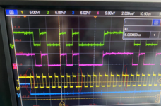
I found if i choose the data out when clk falling, and data in when clk rising , waveform is ok.
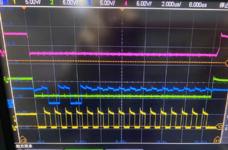
but when I try to choose another mode , data out when clk rising , and data in when clk falling , the waveform is abnormal. You can find some clk wave change the pole every 8bit data transfer. it is very strange.
 

Attachments

  • 2.png
    2.png
    573.9 KB · Views: 121

The waveform suggests that you switching the phase between 8 Bit cycles. This must not happen. Switching clock phase while a SPI slave is enabled is likely to cause transmission errors.

Please show the D2XX API commands you are using to generate the waveform.
 

    james.qiu

    Points: 2
    Helpful Answer Positive Rating
Have you read the FDTI AN_114 document?
What is important with SPI exchanges is to make sure that how you set up the master (the FT2232HL in this - it is always the master) MUST match what the slave is expecting in terms of when data is read by the slave (rising or falling clock edge) from the MOSI line and also when the slave puts valid data on the MISO line. Section 1.2 of the App Note (Page 3) is very clear on when data is valid on the MOSI line and when it expects data to be valid on the MISO line.
NOTE: There is a comment at the bottom of Page 3 of that note that says there are limitations on the CPHA and CPOL combinations that can be used. You will need to check that you are using a valid combination AND that this is also valid for the slave.
Susan
 

    james.qiu

    Points: 2
    Helpful Answer Positive Rating
The waveform suggests that you switching the phase between 8 Bit cycles. This must not happen. Switching clock phase while a SPI slave is enabled is likely to cause transmission errors.

Please show the D2XX API commands you are using to generate the waveform.
hi FvM:
I read the AN_135 FTDI MPSSE Basics Version 1.1, page18, it said :
// Note that since the data in subsequent sections will be clocked on the rising edge, the
//inital clock state of high is selected. Clocks will be generated as high-low-high.


In my application , date is received by slave clock high, so the data out from master will be clock on falling edge. So I initial the CLK port to GND. now the waveform is OK. See the picture 3. Setting SPI in FT2232HL is different from MCU.
--- Updated ---

Have you read the FDTI AN_114 document?
What is important with SPI exchanges is to make sure that how you set up the master (the FT2232HL in this - it is always the master) MUST match what the slave is expecting in terms of when data is read by the slave (rising or falling clock edge) from the MOSI line and also when the slave puts valid data on the MISO line. Section 1.2 of the App Note (Page 3) is very clear on when data is valid on the MOSI line and when it expects data to be valid on the MISO line.
NOTE: There is a comment at the bottom of Page 3 of that note that says there are limitations on the CPHA and CPOL combinations that can be used. You will need to check that you are using a valid combination AND that this is also valid for the slave.
Susan
hi Susan:
thanks for you suggestion, I read the AN_114 again, In my application choose the mode 0x31 (data output on -edge clk, and data in on +edge clk.) it can fullfill slave timing requirement. now the communication is OK. what real confused me is the Pin Initial value configration before and after data sent.
Now I config the CLK=0 CS=0 before data transmit ,then config CLK=0 CS=1 after transmit finished, then it's working.
 

Attachments

  • 3.png
    3.png
    817 KB · Views: 112
Last edited:

Usually the slave doesn't care for initial state of clk line as long as no false active clock edge is generated during transaction start. E.g. the slave can work with SPI mode 0 or mode 3 either.
 

y
Usually the slave doesn't care
Usually the slave doesn't care for initial state of clk line as long as no false active clock edge is generated during transaction start. E.g. the slave can work with SPI mode 0 or mode 3 either.

for initial state of clk line as long as no false active clock edge is generated during transaction start. E.g. the slave can work with SPI mode 0 or mode 3 either.
It seems CLK initial config impact the clk output. even I initial the clk=0 ,befero CLK output, it already pull up.
 

Status
Not open for further replies.

Part and Inventory Search

Welcome to EDABoard.com

Sponsor

Back
Top