Continue to Site

Welcome to EDAboard.com

Welcome to our site! EDAboard.com is an international Electronics Discussion Forum focused on EDA software, circuits, schematics, books, theory, papers, asic, pld, 8051, DSP, Network, RF, Analog Design, PCB, Service Manuals... and a whole lot more! To participate you need to register. Registration is free. Click here to register now.

Flyback converter drawing too much current.

Status
Not open for further replies.

Molectric

Newbie level 6
Joined
Nov 3, 2012
Messages
14
Helped
0
Reputation
0
Reaction score
0
Trophy points
1,281
Activity points
1,417
hello,

i am designing a converter to drive a high power LED(20W). the system has to be a single stage. so i have decided to use the flyback converter. however after building the converter and testing, i seem to draw too much current than expected. My maximum peak input current is 0.2904A from my design and simulations on POWER PSIM. the system i have designed is to be powered by an input voltage ranging from 306V to 338V. a transformer for the flyback converter that i am using is two coupled inductors.
the turns of the coupled inductor are:
Np=96
Ns=7
the inductances are:
Lp=10.53 mH
Ls=0.04842 mH
the length of the air gap:
Lg=0.146 mm

i am using a switch with the ratings, 1000V and 3A(IRFBG30)

the output rectifier diode i am using has the rating 200V and 8A. its an ultrafast diode.
the flyback conveter is suppose to step the voltage down to 20V and the output current is to be 1A.

I am drawing a cuurent of more than 1A at the input at voltages as low as 5V.
if there is anyone who might know the solution to my problem please help as soon as possible.

thanks
 

Since a flyback design is basically a transformer coupled boost inductor, the most common cause of excessive current is transformer saturation.
 
so far i have changed two transformers(coupled inductors) and i am still experiencing the same problem. i have even changed my PCB circuit.
 

Lp=10.53 mH

If the On time is less than 45 uSec, then 300V should push less than 1 A through the coil.

Hence if you set a frequency of 20 kHz or so (at 50 percent duty cycle), then you should get average current of less than 1A through it.

Is 10.5 mH the designed value, or did you measure this as your transformer's real henry value? If it turned out very different from your designed value, then you must alter the frequency and/or duty cycle accordingly.

It also is vital that your switching component turn off completely. Can you verify that it is?

By the way my simulation show an inrush surge up to 10 A in the first 3 mSec after power-up.
 

Lp=10.53 mH is the designed value.
The switching frequency is at 50kHz and the maximum duty cycle is 50% with a minimum of 47.5%.

"It also is vital that your switching component turn off completely. Can you verify that it is?"

No, i don't know what circuit to use to see if my gate driver(HCPL 3120) is able to drive my MOSFET switch well.

"By the way my simulation show an inrush surge up to 10 A in the first 3 mSec after power-up"
The inrush current i did not consider, i only checked my system's behaviour a few seconds later.

On the other hand I will be driving my flyback converter with the power factor correction IC(UC3853), will this function properly?
i have followed the example from Taxas Intruments where a boost converter was used.

i will post my theoretical design and pcb layout for you to check if it is ok.
 

I've been burned by so called "ultra-fast" diodes in the past. Just as a quick and easy check, try disconnecting the output diode (thereby isolating the secondary). If the primary current reduces significantly, then have a closer look at the diodes' switch-off characteristic.

Good luck :)
 
Lp=10.53 mH is the designed value.
The switching frequency is at 50kHz and the maximum duty cycle is 50% with a minimum of 47.5%.

"It also is vital that your switching component turn off completely. Can you verify that it is?"

No, i don't know what circuit to use to see if my gate driver(HCPL 3120) is able to drive my MOSFET switch well.

It will take an oscilloscope to compare voltage drop across the mosfet during On-time versus Off-time.

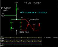
You want low On-resistance and high Off-resistance.

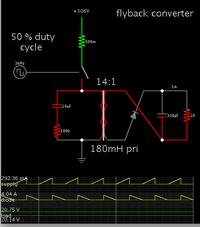
I have made simulations showing the effects.

Very high mosfet Off-resistance:

- - - Updated - - -


Notice the waveform from the supply (top scope trace). Current goes to zero during Off-time.

(To make the waveform easier to observe, I used a slower frequency, and a higher Henry value in the primary.)

----------------------------------

Off-resistance 500 ohms:


Notice that current never goes to zero. Yet you still get 20W to the load.
 

Bradtherad I don't unerstand what to do with the information you gave me. I only understand that with a small on resistance supply current does not go to zero.

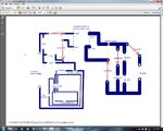
Attached are the circuit diagram i used to simulate on Psim and the pcb i have designed.
is there anything wrong with the my pcb?
i have done it manually because it saves me time since i am new to EAGLE-pcb design tool
Circuit.jpg

PCB.jpg

From the pcb figure, i used wires to measure currents in my system. These wires are represented by jumpers on the pcb figure. The signal from the gate driver(through Rgate resistor) is fine.

i want to know if these connections are correct.
 
Last edited:

I see my images (post #7) disappeared. I plan to re-post my screenshots later because right now they seem to get lost in transfer.

While On-resistance is important (should be very low), your high current draw could come low Off-resistance, that is, from the mosfet not turning off entirely. You say the gate drive is fine, however there may be stray capacitance which slows the mosfet's turning off.

Your schematic looks as though it will work.

When I have attached a full-wave bridge to the secondary, my simulations show the secondary has its greatest current flow while the primary is shut off. (And I have seen the same thing stated in an article.) This can mean that your diode direction makes a big difference.

While you are still in the experimenting stage, I suggest that you see how it affects performance if you attach a full-wave diode bridge. As to waveforms, current draw, net efficiency, coil heating, possible saturation (per post #2), etc.
 
Hey BradtheRad and thylacine1975
I check my circuit over and over. After combining the grounds of the gate drive and that of the main input(one connected to the source of mosfet switch), as done on the HCPL 3120 application circuit, I no longer experienced any overheating of the switch. The circuit was working well.
Another error was with the output rectifier diode. I swapped the diode polarities on my circuit. At the moment I am able to get an output however the voltages are higher than expected. This should be so since I also made a mistake with the number of turns on the original coupled inductor I first built.

Thanks a lot guys.

Good work.

To bring down the output a bit, it still might help to alter the frequency and duty cycle.

My simulation shows there are times when the secondary wants to conduct during On-time, or Off-time, or through the diode one way, or the other way. It is influenced by frequency and duty cycle (though I have trouble determining the relationship). So if the coil energy needs to go somewhere and it sees high impedance, you can get high-V spikes. This is why I recommended a full 4-diode bridge.

Earlier you brought up power factor correction and an IC UC3853. Don't know much about these.
 

Status
Not open for further replies.

Part and Inventory Search

Welcome to EDABoard.com

Sponsor

Back
Top