Continue to Site
Follow along with the video below to see how to install our site as a web app on your home screen.
Note: This feature may not be available in some browsers.
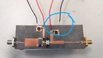
Hi. Thanks for your reply. Want to connect dc power supply to bias common source amplifier. When connect dc power supplies at drain and gate terminals and switch on the dc power supply. The drain side short to the ground.Hi?
What do you want to achieve?
What do you expect?
Generally the Fet's D-S resistance depends on G-S voltage. But G-S is that high impedance that there may exist unknown voltage (due to capacitance and leakage currents). Unknown voltage results in unknown D-S behaviour.
Klaus
After i connect dc sources at drain and terminal sides and switch on dc source. I got short at drain side. So how to properly connnect dc source at drain and gate? VDS 28 V, VGS -3.2Hi,
Still no clear information. It makes it impossible to give good assistance.
-> Use a pen and a sheet of paper and draw what you want to achieve.
There are thousands of hits if you do an internet search on "how to design a common source FET amplifier".
Read through some of them. Choose one that fits you best.Post the link to the document and ask what is unclear.
Klaus
For the first possibility, i am sure that applied negative voltage at gate side with -3.2 V.There are two possiblities:
- You didn't apply a negative bias to the gate, as required for this transistor type, see the explanations in your other thread.
- You see a high drain current despite of a negative bias. Then you have probally killed the FET.
So when do you see it shorted?the current in this case for 28 V at drain with -3.2 V at gate side is IDS= 13 mA
The current observed during simulation. Not measurements. For shorting, once switch on power supplies, it shorted directly at drain side. I have tested the transistor for damaging by measuring gate resistance as recomended by manufactuerer, and got it not damaged.So when do you see it shorted?
Doesn't make much sense, probably wrong simulation setup. Can't assess without seeing the simulation.The current observed during simulation. Not measurements.
Just for confirmation, need to connect power supply at gate side first and switch on. Then, while the voltage is switched on at gate side, i connect the dc at drain side. Am I right?Power supply sequence has been addressed in your other thread. Surely gate bias first.
Doesn't make much sense, probably wrong simulation setup. Can't assess without seeing the simulation.
During the measurements, i got high current 930 mA from dc power supply at the drain side (at the same time voltage at drain side dropped from 28 V to oV), as in the transistor datasheet the current suppose to be 200 mA. What does it mean?Power supply sequence has been addressed in your other thread. Surely gate bias first.
Doesn't make much sense, probably wrong simulation setup. Can't assess without seeing the simulation.