Continue to Site

Welcome to EDAboard.com

Welcome to our site! EDAboard.com is an international Electronics Discussion Forum focused on EDA software, circuits, schematics, books, theory, papers, asic, pld, 8051, DSP, Network, RF, Analog Design, PCB, Service Manuals... and a whole lot more! To participate you need to register. Registration is free. Click here to register now.

Error Timing Analysis Vivado

Status
Not open for further replies.

Moskopole

Newbie
Joined
Apr 26, 2021
Messages
2
Helped
0
Reputation
0
Reaction score
0
Trophy points
1
Activity points
20
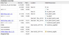
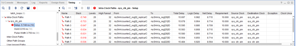
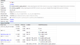
I've been trying to implement a SHA256 design on my Arty a7-35t FPGA. When i try to implement the design, my timing fails wih the following values : WNS: -5.969, TNS : 428. It s my first time encountering this kind of problem and i am not sure how to tackle it. I will post some screenshots under with the error messages that i receive and my Verilog code + testbench .

I've tried adding some pipeline registers but they didnt help, maybe because i dont know where to put them. Thank you in advance.
My code contains the following modules:
1.Uart Receiver
2.SHA 256 parser : adds bits until reaches length of 512
3. SHA256_case: does the hashing
4. UART transmitter
 

Attachments

  • Verilog code + testbench.txt
    13 KB · Views: 109
  • Destination ClockPath.png
    Destination ClockPath.png
    25.1 KB · Views: 164
  • Intra Clock Timing Errors.png
    Intra Clock Timing Errors.png
    45.4 KB · Views: 177
  • Datapath.png
    Datapath.png
    77.1 KB · Views: 147
  • Summary + Source Clock Path.png
    Summary + Source Clock Path.png
    40.4 KB · Views: 174

Your net delays are quite high, they need to be reduced. I guess they are primarily coming from the module SHA256_CASE.
Well you need to analyze a complete failing path. The Datapath.png shows that every computation is adding to the delay. It is here you need to analyze each computation, cut the combinatorial paths and insert registers.
 

all the delay are coming from the SHA256_CASE. I dont quite understand what you mean by cutting the combinatorial paths and inserting registers ? In the case of the Datapath.png should i remove some of the delay type and replace it with a register? To do that, i need to rewrite my code or am i missing something. I am quite confused with this topic? Sorry for asking some maybe basic questions, but i cannot wrap my head around it. Thank you again
 

You are using a bunch of blocking assignments in a edge sensitive always block. This can affect your timing as there is no register for adder outputs, which you then use to perform comparisons or index into an array.

Signals like temp1 are problematic (even without looking at any of your reports, which I haven't looked at) as this is a series of 4 add operations on five 32-bit values, later you add again to produce other values. All of these are assigned in multiple branches of the case statement meaning there is more combinational logic to select the correct logic 'cone' based on the state.

You need to learn the difference between blocking (=) and non-blocking assignments (<=). You can read this presentation on the subject.

I'd bet you have only written software before this. The code looks like you translated an algorithm in C code directly into Verilog and just added a clock around all the logic.
 

Status
Not open for further replies.

Part and Inventory Search

Welcome to EDABoard.com

Sponsor

Back
Top