Continue to Site

Welcome to EDAboard.com

Welcome to our site! EDAboard.com is an international Electronics Discussion Forum focused on EDA software, circuits, schematics, books, theory, papers, asic, pld, 8051, DSP, Network, RF, Analog Design, PCB, Service Manuals... and a whole lot more! To participate you need to register. Registration is free. Click here to register now.

ERROR(ORPSIM-15143): Voltage source and/or inductor loop involving X_U20.L4. You may break the loop by adding a series resistance

Status
Not open for further replies.

EM98

Junior Member level 2
Joined
May 24, 2021
Messages
20
Helped
1
Reputation
2
Reaction score
0
Trophy points
1
Activity points
94
Hi all,
i am facing that problem, any idea ?
1622127338164.png

1622127368377.png

1622127402087.png
 

By grounding terminal 2 and 4 of the symmetrical filter, you are shorting L4 and L8, which isn't permitted for ideal inductors. Please notice that the filter has a hidden ground connection by using node 0 internally. The error message tells how you can bypass the error, but you should sketch the filter circuit with internal ground connection and consider if you really want this topplogy, which doesn't make much sense.
 

Thank you for reply,
Can you please tell me how can i ground internally the filter from the library because i don't know how the elements of the circuit are placed knowing that the lib is generated by spice model generator from s parameters measurements ?
Regards
 

Hi all,
i want to know the input and output of that spice library or how the elements of the circuit are placed, any help ?
1622207266239.png
 

May be the model generator is set to wrong configuration? Apparently the model is for unbalanced 4-port or balanced 2- port device.
 

Exactely i am working on unbalanced 4-port (with forcing a common ground ) / balanced 2- port device.
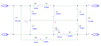
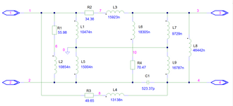
i measured the s-parameters then i generated the spice cirtcuit using ADS.
I used the PI spice model with naraw band spice model generator .
and i am working on a range of frequency of 0-50 MHz.
can you please help that wich generator can i use and how to configure it to get the right spice model ?
--- Updated ---

I really need that
Thank you
 

Your subcircuits "cds" and "IM1" look like this: (see the attached cds_sch.png and IM1_sch.png). Are these topologies really intended?
You can see that within both these subcircuits the global node 0 (earth) is used and at the same time the subcircuit's external (port) pins 2 and 4 are earthed. Using the global node 0 is a very bad practice when creating subcircuits.
Also, some inductances are considered ideal (having no series resistances). This is the cause of your ERROR message ERROR(ORPSIM-15143) concerning L4 within X_U20 (i.e. X_U20.L4); U20 corresponds to the "cds" subcircuit. In my opinion, the same problem with L8 (i.e. X_U20.L8) would follow next (the parser likely shows just the first discovered error).
 

Attachments

  • cds_sch.png
    cds_sch.png
    28.8 KB · Views: 122
  • IM1_sch.png
    IM1_sch.png
    30 KB · Views: 96
Global port 0 can make sense if the circuit models an unbalanced 4-port device. EM98 didn't tell which s-parameter file type has been imported.
 

Here is my approach :
i am working on creating a simulation model of the BCI test. to model the PCB in the simulation circuit i have to measure the s-parameters of my DUT (balanced 2 port/unbalanced 4 port) with the VNA (BODE 100) to generate the touchstone files (S2P), after that i combined the s2p files (6 files) with the touchstone combiner (ADS) to get an S4P file and from that file i have to generate a spice model (narawband generator, PI ) so the library file is generated automaticly the when it's implemented into the simulation model i get this error.
i guess if i change some thing in the library(deleting the the node 0) i will change the PCB release presentation.
any advice about the hole approach or how to generate the right spice model to be implemented in the circuit below ?
Test frequency range : 0-400MHz but i have i limitation due to frequecny range of the vna so i am working in a range of 0-50Mhz
signal transfer : for s-parameters probing
Thanks
1622293042238.png
 

Your simulation circuit uses unbalanced 2-port connection, the appropriate s- parameter description is single s2p. Floating internal ground node will completely change the behaviour. If you want to short two inputs of your model to ground, you can add small dummy resistors (e.g. microohm range) to the grounded inputs and the simulator should accept the circuit.
 

I have a transmission line in the circuit which represents the my twisted harness (+data,-data) so it's a balanced 2 port simulation circuit,
then i have my dut(4port unbalanced ciruit) and while working with a 2 port VNA i have to generate aS2P files to be combined in order to get the standards s-parameters matrix so i have to use S4P file.
while i cant change anything in the library file generated and getting this error, can i add a dummy resistor (e.g. microohm range) ? it's will not impact the original behavior ? because i have to keep it.
this what i have done and it's works
1622305932474.png

1622305977829.png
 

You understand that grounding U20.2 or not makes a difference? Similarly, grounded U20.4 doesn't seem to fit the s-parameter model. These points are however beyond the original question. The simulation error is solved by the suggested method, but I seriously don't know if the simulation is corresponding to the modelled real world problem.
 

Status
Not open for further replies.

Part and Inventory Search

Welcome to EDABoard.com

Sponsor

Back
Top