Continue to Site

Welcome to EDAboard.com

Welcome to our site! EDAboard.com is an international Electronics Discussion Forum focused on EDA software, circuits, schematics, books, theory, papers, asic, pld, 8051, DSP, Network, RF, Analog Design, PCB, Service Manuals... and a whole lot more! To participate you need to register. Registration is free. Click here to register now.

Electrical line distance vs phase shift

enemra

Junior Member level 1
Joined
Oct 19, 2011
Messages
19
Helped
0
Reputation
0
Reaction score
0
Trophy points
1,281
Activity points
1,440
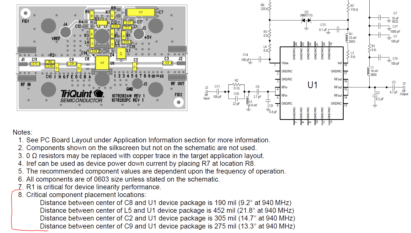
The below screenshot is from TQP7M9104 page-8. Note 8 provides the constraints on the distance between components. If I am not wrong, this is for electrical line distance to control the phase offset. I have two questions wrt this.

1. How can we actually calculate this phase shift for the placement of specific component? Any tool or any pointers to where I can learn?

2. This component is an amplifier and how did the manufacturer come at the number 9.2 deg, 21.8 deg, 14.7 deg, etc?
1686065253999.png


Thanks in advance
Enemra
 
Δϕ = 2π * (ΔL / λ)
where Δϕ is the phase shift, ΔL is the difference between the physical lengths of the transmission (delay) line, and λ is the guide wavelength.
 
hmmm. "phase shift"?

indeed there is phase shift associated with added line length. but it seems like you are looking at this from the wrong perspective.

Lets postulate an amplifier. It does not have a 50 ohm output impedance. Using various design apps, or a smith chart, you figure out it wants a 1 pf shunt capacitor, followed by a 2 pf series capacitor, to make it matched to 50 ohms at the output connector. but you do not know WHERE to physically place those components.

So you enter the ouput impedance information (usually in an s2p file) into a simulation program, you add a legth of 50 ohm microstrip at the output pin running to the 1 pf shunt capacitor. You model the T junction where the capacitor attaches, and the via hole connecting the capacitor to the ground plane. then you add another 50 ohm length of microstrip leading to the 2 pf series cap. you model the solder pads that series cap uses also. then you run the simulation. look at gain vs frequency, and output match vs frequenecy.

IF it is good enough, bingo, you make the artwork. IF NOT good enough, you try varying the 1 and 2 pf capacitor values slightly, you try varying the two lengths of microstrip line, you maybe try using non 50 ohm lengths of line. and so on. when it looks good enough, maybe it is slightly changed, but now work fine over the bandwidth you need.

the key is to know the S parameters of that triquint chip, and model the microstrip elements properly.

without doing the simulation, you can take a guess at things, keeping the two transmission lines small as possible, and be prepared to physically TUNE the amplifier up in the lab to try to get it to work
 
I think things are much simpler. The manufacturer gives these physical and electrical lengths just to understand how to make the PCB layout.
Actually the distances between components are wrong presented, and don't make any sense to be all of them referenced to U1.
From impedance matching point of view, they should be presented as independent TL stubs and their lengths should not be referenced to U1 device.
Only one distance should be referenced to U1 and this is the distance from C8 to U1. All the others should be given as: distance between C8 and C9, distance between C9 and L5, etc.
Doing a quick TL simulation, the substrate used in the design have Er = 3.7. With this Er you get a match between physical and electrical lengths at 940MHz as shown in the picture.
 
If only the capacitance or inductance is used to adjust the phase shift,then the capacitance to ground phase shift decreases and the inductance to ground phase shift increases.
 

LaTeX Commands Quick-Menu:

Similar threads

Part and Inventory Search

Welcome to EDABoard.com

Sponsor

Back
Top