you23
Newbie level 3
Hi,
I designed 2nd order sigma-delta modulator (1bit), and made chip, and measuring now.
I use FPGA after modulator output. the FPGA is used for sinc3 decimation filter (16bit out).
I have a distortion problem for measurement.
test condition;
VDD=3V, VSS=0V, VREF+=3V, VREF-=0V, VCOM=0.4*VDD(from external)
fclk=100k, 250k, 500k from external generator.
I use 16bit DAC and buffer amplifier(VDD=5V, VSS=-5V) for input.
Sweep this DAC level from 0 to VDD. (I checked good result(linerlity) by using other ADC).
Sweep DAC level:
puluse input : 0 to VDD (full scale)
minus input : common (0 or VDD/2 or VDD)
Detail of problem;
No change in fclk(100k to 500k), VDD(2V to 4V), minus input level(0 or VDD/2/ or VDD).
When I change input pulse and minus, I got save result.
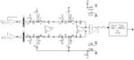
I made two chip. these difference is switch size.
one is 1:1 switch (NMOS 2u/1u : PMOS 2u/1u) for all transmission switch.
another is 1:3 switch (NMOS 3u/1u : PMOS 9u/1u) for all transmission switch.
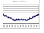
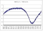
for these chip, INL curve is different. (attach graphes below)
I measured 5 pics for each chip. and these are same trend bud level is a little different.
And This INL does not occur in simulation (BSIM3.22, level 49, HSPICE)
I have not tried post layout simulation, but I inted to care for near hi-impedance lines....
pleasae advice me.
I designed 2nd order sigma-delta modulator (1bit), and made chip, and measuring now.
I use FPGA after modulator output. the FPGA is used for sinc3 decimation filter (16bit out).
I have a distortion problem for measurement.
test condition;
VDD=3V, VSS=0V, VREF+=3V, VREF-=0V, VCOM=0.4*VDD(from external)
fclk=100k, 250k, 500k from external generator.
I use 16bit DAC and buffer amplifier(VDD=5V, VSS=-5V) for input.
Sweep this DAC level from 0 to VDD. (I checked good result(linerlity) by using other ADC).
Sweep DAC level:
puluse input : 0 to VDD (full scale)
minus input : common (0 or VDD/2 or VDD)
Detail of problem;
No change in fclk(100k to 500k), VDD(2V to 4V), minus input level(0 or VDD/2/ or VDD).
When I change input pulse and minus, I got save result.
I made two chip. these difference is switch size.
one is 1:1 switch (NMOS 2u/1u : PMOS 2u/1u) for all transmission switch.
another is 1:3 switch (NMOS 3u/1u : PMOS 9u/1u) for all transmission switch.
for these chip, INL curve is different. (attach graphes below)
I measured 5 pics for each chip. and these are same trend bud level is a little different.
And This INL does not occur in simulation (BSIM3.22, level 49, HSPICE)
I have not tried post layout simulation, but I inted to care for near hi-impedance lines....
pleasae advice me.