Continue to Site

Welcome to EDAboard.com

Welcome to our site! EDAboard.com is an international Electronics Discussion Forum focused on EDA software, circuits, schematics, books, theory, papers, asic, pld, 8051, DSP, Network, RF, Analog Design, PCB, Service Manuals... and a whole lot more! To participate you need to register. Registration is free. Click here to register now.

[SOLVED] direct PWM to MOSFET

Status
Not open for further replies.

P.Copper

Member level 5
Joined
Mar 18, 2013
Messages
82
Helped
0
Reputation
0
Reaction score
0
Trophy points
1,286
Activity points
1,807
Hi y'all

I'm trying to drive the MOSFET directly with the PWM. I generated a PWM signal using dspic30f4011 and because the MOSFET needs atleast 10V to switch on. I then used a MOSFET gate driver (HCPL 3120) to boost the voltage.

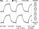
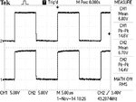
I get a nice clean gate signal but immediately when i connect the PWM signal to the MOSFET the gate signal changes from this F0002TEK.JPG to thisF0003TEK.JPG. can someone help me with this. Thanks
 

"A" MOSFET could be anything from a couple hundred pF to
tens of nF load at the FET driver output. You should have at
least 10X Cgg as close-in decoupling at the driver and probably
this should be a 1X low-ESR/ESL and a 10X bulk cap.

I do not see the usual "porch" about mid-swing and so suspect
that the MOSFET does not have -its- load, yet.

MOSFETs don't need 10V to switch on; they need (old ones,
anyway) 10V to have Ron fully driven to minimum. VT is more
likely 3-4V.

I recommend you play with LTSpice or TINA, depending on
which one might have the closest and best model for the
driver and FET in question. See what a simple lashup shows
for the same probe-points and conditions.

To me this only looks like too much capacitive load for the
drive strength of the FET driver. Which may or may not be
the driver's fault entirely - is your board holding up its end,
especially regarding power and ground trace resistances?
 

This is because of "Gate Capacitance" and "Series Resistance" on the path if there are some resistive elements on the road.It's typical R-C time domain response and you should use a buffer which is capable to drive this capacitive gate.Because of signal generator impedance and unsufficient driving capabilities of the generator the waveform is shaped..
 

Which MOSFET? Any external Rg connected? Without this information, your post is about to useless.
 

1. Your drive has a very short risetime, have you worked out the DV/Dt, then apply this to the input capacity of the FET, hence you can find the charging current. Where is this charging current coming from?
2. The waveform on the FET gate shows a CR time constant of about 2.5µ S (100%Vg @ 10µS). we know where the C is coming from what about the R?.
From 1 does the supply to the driver dip? from 2 is there some series resistor to the FET gate?
Frank
 

What are these TWO traces of ? Are these 2 separate signals each driving a mosfet or what ?
 

The Agilent Mosfet driver does not have enough output current to quickly charge and discharge the high gate-source capacitance of your Mosfets at 49kHz. It will be much better at 4.9kHz but then you will hear it.
 

What are these TWO traces of ? Are these 2 separate signals each driving a mosfet or what ?

no, the first trace is the gate signal before i connect it to the mosfet, the second is after connecting it

- - - Updated - - -

Which MOSFET? Any external Rg connected? Without this information, your post is about to useless.

i'm using IRFB4229Pbf
 

The capacitance of your Mosfet is very high. You need a gate driver that provides much more current to drive it quickly.
 

I do have a gate driver circuit, i used the HCPL 3120 gate driver but the problem still persists. how much more current specifically? the HCPL that i'm using gives out 2A.
 
Last edited:

Are you testing the circuit on a solderless breadboard that has contacts that cannot pass 2A of current to the gate?
Then the contacts and wiring are resistors that slow down the risetimes and falltimes.
 

The oscilloscope plots show the "classic" resistance-capacitor charging and discharging waveforms from a squarewave source.

You have way too much an R*C product for the switching frequency.

Since most likely the "C" is fixed by your Mosfet, you have to lower "R"...as simple as that.

So the question is:
-Is there any series resistance anywhere, and that includes stray resistance, and the gate driver's power supply resistance?
 
The IRFB4229Pbf driver appears to be able to deliver adequate current to drive the MOSFET capacitance to give less than a 100nS rise-time so there appear to be some external resistance in the circuit, as others have noted.

Post your schematic.
 

Almost every time there is a problem with a circuit it is a solderless breadboard that is the culprit.
But maybe the Mosfet driver IC is in one city and the Mosfet is in another city?
 

The oscilloscope plots show the "classic" resistance-capacitor charging and discharging waveforms from a squarewave source.

You have way too much an R*C product for the switching frequency.

Since most likely the "C" is fixed by your Mosfet, you have to lower "R"...as simple as that.

So the question is:
-Is there any series resistance anywhere, and that includes stray resistance, and the gate driver's power supply resistance?

Oh shoot!!!! for some reason I used a 270ohm resistor instead of a calculated 5.6 ohm resistor..

- - - Updated - - -

Are you testing the circuit on a solderless breadboard that has contacts that cannot pass 2A of current to the gate?
Then the contacts and wiring are resistors that slow down the risetimes and falltimes.

I'm testing it on a vero board, i'm not sure but i think i can handle up to 3A if i'm not mistaken. I stand to be corrected!
 

Thanks y'all problem solved by decreasing the resistance.
 

Status
Not open for further replies.

Similar threads

Part and Inventory Search

Welcome to EDABoard.com

Sponsor

Back
Top