Continue to Site

Welcome to EDAboard.com

Welcome to our site! EDAboard.com is an international Electronics Discussion Forum focused on EDA software, circuits, schematics, books, theory, papers, asic, pld, 8051, DSP, Network, RF, Analog Design, PCB, Service Manuals... and a whole lot more! To participate you need to register. Registration is free. Click here to register now.

Digital pot X9C102 terminal voltage problem.

Status
Not open for further replies.

Gigillo74

Member level 3
Joined
Aug 24, 2007
Messages
61
Helped
0
Reputation
0
Reaction score
1
Trophy points
1,288
Location
Bologna - Italy
Activity points
1,662
Hi all,
i've a problem to solve with maximum pot terminal voltage.
I need to work with +-8V to VH and VL terminal but max applied voltage is +-5V.
Someone have a solution to increase this max value using external components?
Thank You.
Luigi
 

there’s no way to change the specifications for a device. if the maximum voltage is 5 volts, then it’s 5 volts. you can add external resistors, but that will lower your range to +/-5.
Maybe tell more about your application.
 
Hi,

Yes, like how much current (a numerical value) will pass through the trimpot?

A simple resistive divider might be all you need in the best of cases, ratio of Rtop = 0.375, Rbottom = 0.625. If you know the current in Amps the +-8V has to pass through the trimpot, you can calculate the decade minimum/maximum of resistor (kilo, Mega, etc) the Rtop, Rbottom pair will need to be that is ideal to provide enough - but not too much as wasted energy - current for whatever the trimpot goes to.
Another way is attenuating the +-8V signal with an op amp.
 

Thank you very much for reply.
I'll post the sch where pot.is used.
It is used as feedback on pin 2 of L200 to set current.
The maximum working current of the pot is 10mA.
 

HI,

using a pot in the "current limiter" circuit i counter productive

The current limiter becomes active with a voltage difference of 0.45V between pins 2 and 5.


Example: If you want to be able to adjust the limit 100mA ... 1A, then
You need to install a shunt (resistor) for the lower current --> 0.45V / 0.1A = 4.5 Ohms.

At pot = 100% you get a limit of 100mA
At pot = 10:1 (10%) you get a limit of 1A
To get 1A limit you need to divide the voltage of the 4.5 Ohms shunt down 10:1.
So the IC works with 0.45V, the voltage across the shunt then is 4.5V

This causes some problems:
* 4.5W of power dissipation in the shunt
* 4.5V of additional voltage drop .. thus the usable output voltage is decreased.

****
I guess you find solutions for this problem in the internet.

My L200 approach: calculate the shunt value for the maximum current range.
* add a 100 ohms resistor from shunt to pin 2
* add an adjustable current sink to pin 2: 0...4.5mA (for 100% down to 0% of load current)
(adjustable via pot)
Working principle:
The 0..4.5mA causes an (additional to load current) of 0...450mV at pin2. For the L200 this looks like load current.
Example: 3mA causes 300mV of voltage drop at the 100 Ohms resistor, thus the L200 current limiter gets activated at (450mV - 300mV) 150mV of shunt voltage.

On the other hand: we currently have switch mode regulators to avoid high power loss and high heating.

Klaus
 
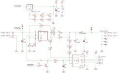
This is my circuit.
To reduce voltage across pot terminals, i think i need another resistor after pin 3 of digital pot.
 

Attachments

  • l200.png
    l200.png
    98.9 KB · Views: 119

Hi,

I might be wrong, an op amp buffer between L200 Out and the digi-trim-pot may prove helpful, or is the X9C102 high impedance input and enough to not steal current from L200 Out signal?
 

Hi,

I might be wrong, an op amp buffer between L200 Out and the digi-trim-pot may prove helpful, or is the X9C102 high impedance input and enough to not steal current from L200 Out signal?
The main X9C102 issue in this circuit is max voltage between pin 3-6 that exceded max value. to reduce this voltage and make able pot to feedback on L200 i think a resistor need to be added in series of pin 3.
 

Again, I may be wrong but the suggestion of a resistor, and only there to burn up heat on a sensitive node, causes me marginal distress ;). Maybe it's fine. An op amp high impedance input buffer that attenuates instead of amplifies is also do-able there.
 

Again, I may be wrong but the suggestion of a resistor, and only there to burn up heat on a sensitive node, causes me marginal distress ;). Maybe it's fine. An op amp high impedance input buffer that attenuates instead of amplifies is also do-able there.
Ok, thank you.
I'll try to update the sch and after i'll post the new one.
 

Hi Gigillo74,

Can you walk me through a couple of things in/about your circuit, please? I'm pretty ignorant, really, I mean it... I'd hate to give you useless suggestions about op amps you may not need.

My limited understanding:
* L200 is the (voltage and/or current?) regulator in a charger circuit which has two selectable current limit preset options (15R or 3.3R).
* L200 will be externally set via code (R/W, etc.) by you at xyz wiper voltage to be able to dynamically select L200 output current limit.
* The X9C102 isn't going to use 10mA from the L200 output line at all, in fact it's probable that it will only use a minimal amount of current because it is only a feedback sensing device. It can handle a maximum of +-4mA at either input (H or L), but you have no reason/need to force +-8mA through it for your purposes (much less 10mA). I only read the datasheet quickly but don't understand the need for maximum current at pin 6 (Low) e.g. 1.8k resistor (8V/1.8k = 4.4mA) and no current limiting at pin 3 (High).
* L200 pin 6 (Low) - after the 1.8k resistor is that going to see 0V continuously or what voltage do you expect there?
* Why does the X9C102 pin 3 (High) need to be powered from the L200 output? Why is pin 6 (Low) not connected to ground? I assume both questions are answered by saying that they are a part of the dynamic feedback set-up for this circuit for it to function correctly, but I am too stupid and lazy to try to undestand what's going on there.
* Does your circuit actually use a negative voltage or current anywhere at all? From the schematic I can only see +5V and GND. There is no -5V, or -8V anywhere, neither a power supply nor a reverse signal that could generate a 'negative' value (such as a bi-directional battery charger circuit that has charger current in and load current out sampled on the same path).
* Do you think adding an attenuating op amp buffer between L200 Out and digipot High to subtract those excess 3V is useful or is just adding an unnecessary additional IC where Rdiv alone is actually enough of a solution?

Anyway, to save you laborious time answering so many (pointless, and clueless) questions:

Now that I think I understand what I think I understand about your circuit, and I doubt losing a few uA or even mA here or there along the charger out path matters because the charging current (8V/15R = 0.533A; 8V/3.3R = 2.424A) is large in comparison to the maximum digipot current, maybe you are right and a simple resistive divider is more than acceptable - so long as it doesn't distort the feedback to the L200.
And looking at the L200 output impedances you have (15R or 3.3R), even RdivTotal = ~800R for ~10mA + digipot current, guessing that the load to be charged must also be pretty low impedance as an input given the 0.5A or 2.4A, then the 8V>5V divider could be 800R (0.625 x 800R = 500R) at e.g. 500R x 0.01A^2 = 50mW. Rtop = 300, Rbottom = 500. 30mW and 50mW, not so bad, surely? Using 3k and 5k would mean 1mA through the divider and 3mW and 5mW on each resistor. I haven't considered the implications of placing 500R fixed resistor to ground directly in parallel with a variable 1k to ground, though, might get some interesting voltages there that are not 5V precisely and again distort/warp/skew the feedback signal.
 

Hi again,

You really have +-8V, do you? I ask as I realised (one of) the 'flaw(s)' in my suggestion, which is that a non-inverting amplifier is always Vo = R2/R1 +1, so as that is unworkable mathematically, it only really leaves my toolbox with: single supply solution [buffer + rdiv + buffer] or dual supply solution [inverting amplifier with its helpful Vo = -R2/R1 + another inverting amplifier to turn negative back to positive...]. If you don't already have a negative supply, then the inverting amplifier solution is (maybe necessary but) unappealing just because it means more parts and effort and PCB space.

Here is a quick sim of the inverting amplifier version. It's clunky/would take up more space than you might be happy with, compared to a resistive divider alone. The resistive divider version simulation was unconvincing for me. So, again, for a resistor to drop a few mW dissipating e.g. 3V at what I still assume is negligible current into the digipot High pin, even 10mA across a 3k resistor would only be 0.3W.

Sim results just meant to give idea of what I thought might work as a solution, and as orientative because e.g. L200 is an IC, not a 0 Ohm impedance voltage source, and e.g. Vout OA at 5.001V is amusingly too-perfectly accurate for reality...

eda Gigillo74.JPG
 

Hi d123,
thank you for your time in reply.

* L200 is the (voltage and/or current?) regulator in a charger circuit which has two selectable current limit preset options (15R or 3.3R).
Yes, it is.

* L200 will be externally set via code (R/W, etc.) by you at xyz wiper voltage to be able to dynamically select L200 output current limit.
Yes, i would to do it but not dinamically. Only set current charge by dig pot.
* The X9C102 isn't going to use 10mA from the L200 output line at all, in fact it's probable that it will only use a minimal amount of current because it is only a feedback sensing device. It can handle a maximum of +-4mA at either input (H or L), but you have no reason/need to force +-8mA through it for your purposes (much less 10mA). I only read the datasheet quickly but don't understand the need for maximum current at pin 6 (Low) e.g. 1.8k resistor (8V/1.8k = 4.4mA) and no current limiting at pin 3 (High).
Yes also for this. It is not necessary to force any current. I need only a voltage from pin 5 to shunt resistor to feedback into pin 2 to regulate constant current. The idea is to place a parallel dig pot instead a manual pot (just working with this solution) to regulate charge current. Output voltage is not defined. It adjust itself automatically in funcion of type of battery is connected.
* L200 pin 6 (Low) - after the 1.8k resistor is that going to see 0V continuously or what voltage do you expect there?
The 1,8K resistor is used as voltage divider to make dig pot max voltage low to 5v.
* Why does the X9C102 pin 3 (High) need to be powered from the L200 output? Why is pin 6 (Low) not connected to ground? I assume both questions are answered by saying that they are a part of the dynamic feedback set-up for this circuit for it to function correctly, but I am too stupid and lazy to try to undestand what's going on there.
Pin 3 must have some resistor as pin 6 to complete the voltage divider. Only forgot to put it in sch.
* Does your circuit actually use a negative voltage or current anywhere at all? From the schematic I can only see +5V and GND. There is no -5V, or -8V anywhere, neither a power supply nor a reverse signal that could generate a 'negative' value (such as a bi-directional battery charger circuit that has charger current in and load current out sampled on the same path).
No, any negative voltage. Power supply is 12V
* Do you think adding an attenuating op amp buffer between L200 Out and digipot High to subtract those excess 3V is useful or is just adding an unnecessary additional IC where Rdiv alone is actually enough of a solution?
If i know how to insert it in the circuit, the reply is yes.
Anyway, to save you laborious time answering so many (pointless, and clueless) questions:

Now that I think I understand what I think I understand about your circuit, and I doubt losing a few uA or even mA here or there along the charger out path matters because the charging current (8V/15R = 0.533A; 8V/3.3R = 2.424A) is large in comparison to the maximum digipot current, maybe you are right and a simple resistive divider is more than acceptable - so long as it doesn't distort the feedback to the L200.
And looking at the L200 output impedances you have (15R or 3.3R), even RdivTotal = ~800R for ~10mA + digipot current, guessing that the load to be charged must also be pretty low impedance as an input given the 0.5A or 2.4A, then the 8V>5V divider could be 800R (0.625 x 800R = 500R) at e.g. 500R x 0.01A^2 = 50mW. Rtop = 300, Rbottom = 500. 30mW and 50mW, not so bad, surely? Using 3k and 5k would mean 1mA through the divider and 3mW and 5mW on each resistor. I haven't considered the implications of placing 500R fixed resistor to ground directly in parallel with a variable 1k to ground, though, might get some interesting voltages there that are not 5V precisely and again distort/warp/skew the feedback signal.
3k & 5k are most interesting solution
--- Updated ---

Hi again,

You really have +-8V, do you? I ask as I realised (one of) the 'flaw(s)' in my suggestion, which is that a non-inverting amplifier is always Vo = R2/R1 +1, so as that is unworkable mathematically, it only really leaves my toolbox with: single supply solution [buffer + rdiv + buffer] or dual supply solution [inverting amplifier with its helpful Vo = -R2/R1 + another inverting amplifier to turn negative back to positive...]. If you don't already have a negative supply, then the inverting amplifier solution is (maybe necessary but) unappealing just because it means more parts and effort and PCB space.

Here is a quick sim of the inverting amplifier version. It's clunky/would take up more space than you might be happy with, compared to a resistive divider alone. The resistive divider version simulation was unconvincing for me. So, again, for a resistor to drop a few mW dissipating e.g. 3V at what I still assume is negligible current into the digipot High pin, even 10mA across a 3k resistor would only be 0.3W.

Sim results just meant to give idea of what I thought might work as a solution, and as orientative because e.g. L200 is an IC, not a 0 Ohm impedance voltage source, and e.g. Vout OA at 5.001V is amusingly too-perfectly accurate for reality...

View attachment 178915
Thank you for this sample. I've reply to all question in previous post. If you confirm it as good solution, i'll try to check the ckt building it.
 
Last edited:

Hi,

first time you tell you want to build a charger.
Why don´t you use a dedicated charger IC ... with interface to control the charging parameters?

Nowadays I´d not use a linear charger. Low efficiency, much dissipated heat...

Dedicated charger ICs are designed to charge battries... with all it´s benefits and more features than a L200 can give.

Klaus
 

If you confirm it as good solution, i'll try to check the ckt building it.
Hi,

Thanks for all the information you provided.

Caveat emptor, please, it's only a possible solution - but you still need to check it first as valid, either by doing a little bit of maths and then a few simulations under different circuit conditions (and assessing the credibility of the simulated results) and/or a little bit of maths and then breadboarding it before soldering anything.

I'd try the simple 3k-5k divider first, if changing the digipot resistance value alters the 5V coming from the 3k-5k divider, then a buffered approach as shown above might be next-best option.
 

I'd try the simple 3k-5k divider first, if changing the digipot resistance value alters the 5V coming from the 3k-5k divider, then a buffered approach as shown above might be next-best option.
Perfect, i'll do it. I will update you.
Thank You for all suggestions.
 
Hi,

Thanks for all the information you provided.

Caveat emptor, please, it's only a possible solution - but you still need to check it first as valid, either by doing a little bit of maths and then a few simulations under different circuit conditions (and assessing the credibility of the simulated results) and/or a little bit of maths and then breadboarding it before soldering anything.

I'd try the simple 3k-5k divider first, if changing the digipot resistance value alters the 5V coming from the 3k-5k divider, then a buffered approach as shown above might be next-best option.
Hi,
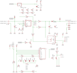
i've try to add resistors as you have suggested and the circuit works fine.
Now i need to make it more sensitive because if there is a 9V battery as load the voltage drop on low value R is small and so the feedback doesn't have best resolution.
The working schematics is this:
 

Attachments

  • L200-new.jpg
    L200-new.jpg
    657.6 KB · Views: 101

Hi,

I'm glad to hear you have it working.

I believe that you need to make the 3k into 4k. 5/9 = 0.555. 5000/9000 = 0.555r. 0.555r * 9V = 4.995V.

If so, same as you have the 3.3R and 15R with switches. You could e.g. parallel one of R6 or R11 with a 2.5k (2k2 + 330R) for when Vbat is 9V.

I think, at first look. Hope that's what you mean.
 

HI,

I can´t see why now in the schematic of post#17 the voltage levels for the pot should be within specified range.
Did you measure it?

Also I don´t understand the series connections of several resistors.
please explain.

Klaus
 

Status
Not open for further replies.

Part and Inventory Search

Welcome to EDABoard.com

Sponsor

Back
Top