Continue to Site

Welcome to EDAboard.com

Welcome to our site! EDAboard.com is an international Electronics Discussion Forum focused on EDA software, circuits, schematics, books, theory, papers, asic, pld, 8051, DSP, Network, RF, Analog Design, PCB, Service Manuals... and a whole lot more! To participate you need to register. Registration is free. Click here to register now.

Digital Design Basics: T FF from D FF

Status
Not open for further replies.

David83

Advanced Member level 1
Joined
Jan 21, 2011
Messages
410
Helped
45
Reputation
92
Reaction score
45
Trophy points
1,308
Activity points
3,639
Hello all,

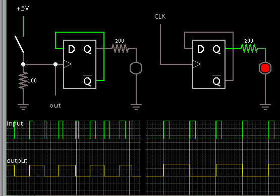
My question is very basic: I'm reading a book on Verilog HDL, and at some point the author said that we can build a T flip-flop from a D flip flop and inverters, where the output of the D FF is negated and fed as an input. However, this results in a characteristic table that is the opposite of the T FF, namely, if T=1 then the output is held, and if T=0 the the output is toggled.

Did I miss something here? Isn't the characteristics of T FF is as following: if T=0 then hold (the current state), if T=1 then toggle? Is positive or negative edge triggered flip flops has any effect here?

Thanks
 

A toggle flip flop can be thought of as a divide-by-2. (Push-on, push-off.)
The D flip flop is easily transformed into a divide-by-2.
 

A toggle flip flop can be thought of as a divide-by-2. (Push-on, push-off.)
The D flip flop is easily transformed into a divide-by-2.

OK, I used to know more on digital designs, but I have been out of touch for many years now. So, could you explain to me how to build a T FF from a D FF and an inverter in a more detailed way?
 

At left is the toggle FF. At right is the divide-by-2 FF. They act the same way.


The inverting gate does not seem necessary, although it can be used to make the output transition at the trailing edge instead of the leading edge. Anyway there's the chance I didn't grasp the particular concept which the author had in mind.

This is the schematic and the characteristic table from the book


TFF.png
 

This is the schematic and the characteristic table from the book


View attachment 131890

This "truth" table really confuses me. I'm wondering if this is some new fangled T flip-flop that I've never heard of?

Here is an example of what I learned back in school . Note the T flip-flop does not have a truth table that looks like:
Code:
reset  qn | qn+1
----------+-----
  1     1 |  0
  1     0 |  0
  0     0 |  1
  0     1 |  0
  0     0 |  0
What is up with these lines
Code:
0   0 | 1
0   0 | 0
How can you have two sets of present states generate a next state that is different? Seems more like very "Fuzzy Logic" to me ;-)

Code:
 t  qn | qn+1
-------+-----
 0   0 |  0
 0   1 |  1
 1   0 |  1
 1   1 |  0
This is the traditional T flip-flop that I learned in school and appears to be the same as what is being taught at Univeristy of Maryland (the link).

- - - Updated - - -

update....

Maybe it's just morbid curiosity, but what is the title of that book and who wrote it?
 

It confused me as well. This is the book.
 

Interesting I never noticed that.

BTW I have that book (2nd edition instead of 1st) and found the same Figure 2-4 in my copy. I never noticed it before since I never even looked at the first 3-4 chapters. I actually learned Verilog from the Thomas & Moorby book and only picked up the Palnitkar book as the other book was outdated and reading the LRM too many times puts me to sleep ;-)

- - - Updated - - -

If that truth table and circuit can do what it claims then I think we have a truly random random bit sequence generator :-D.

I think it generates the invert of the T FF, doesn't it? (Don't use the characteristic table, just build one from the schematic figure)

By the way, I'm trying to learn hardware design, and I think Verilog HDL is necessary for that. Could you guide me to a free software and may be an easy tutorial to begin with? I'll read the theory in parallel (I have some digital design background, and I think I can understand a tutorial).

Also, just to get the big picture to make sure I'm learning something valuable in the job market: in my undergrad I took courses on computer architecture, digital logic design, and VLSI. I think all of these have a role on hardware design. Are these separate steps, and what's the goal of each step?

Thanks
 

I think it generates the invert of the T FF, doesn't it? (Don't use the characteristic table, just build one from the schematic figure)
It was a joke about the table being wrong, I know the schematic is an inverted T FF. BTW, if you put an inverter in the "reset" it will act like a normal T FF.

By the way, I'm trying to learn hardware design, and I think Verilog HDL is necessary for that. Could you guide me to a free software and may be an easy tutorial to begin with? I'll read the theory in parallel (I have some digital design background, and I think I can understand a tutorial).
Well Verilog or VHDL are used to implement ASIC/FPGA designs, but if you design stuff onto a PCB then you will also use ICs. Well Altera has a web version of Quartus that allows you to work on their FPGAs and Xilinx has ISE 14.7 (for devices before 7 series) and Vivado for 7 series and newer devices (but I think the sign up to get the webpack version requires a corporate email address, i.e. gmail won't work)

Also, just to get the big picture to make sure I'm learning something valuable in the job market: in my undergrad I took courses on computer architecture, digital logic design, and VLSI. I think all of these have a role on hardware design. Are these separate steps, and what's the goal of each step?

Thanks
I wouldn't call them steps of a design process, but the first two are usually done as architect something (big picture designing), digital logic design (implement the details of the design). VLSI is just Very Large Scale Integration and kind of encompass the entire development of an IC from conceptualization-architecture-implementation-verification-manufacturing.

computer architecture - how to structure a computer to do something useful, e.g. processor connected to frontside bus, frontside bus connected to memory/peripherals etc, or a processor with multi-cores, etc.
digital logic design - so you know how AND/OR/XOR/etc gates work and the transformations you can do to boolean equations along with understanding FF, multiplexers, etc and hooking all of these up and understanding how to do timing analysis on a circuit to see if it will work.
VLSI - ASIC design, and FPGA design if you consider how big FPGAs have become since the term VLSI was coined.
 

My understanding is that the reset input is used to reset the output to 0 regardless of the current state, isn't it?

Thanks for explaining the differences between computer architecture, digital logic design, and VLSI. So, can I skip computer architecture and go to the digital logic design, or I need to go through the architecture first?

As I understood, VLSI is the implementation of the higher level designs, right?
 

My understanding is that the reset input is used to reset the output to 0 regardless of the current state, isn't it?
I suppose that is true in this instance, the drawing really isn't a T flip-flop as there is no T input to toggle the output. I think the author really dropped the ball on Fig 2-4.

Thanks for explaining the differences between computer architecture, digital logic design, and VLSI. So, can I skip computer architecture and go to the digital logic design, or I need to go through the architecture first?

Skipping the "design" of the architecture is the reason I've seen many designs that look like a steaming pile of poo, that don't even meet the design's performance requirements.

As I understood, VLSI is the implementation of the higher level designs, right?
No, never said that, it's basically large scale chip design...
In the early days it was
Transistors
SSI - single or multiple AND/OR/XOR/etc gates on one die
MSI - things like 4-bit arithmetic ICs, counters, multiplexers, lots of gates on one die making up a function
LSI - CPUs like the venerable 8051 or things like TRW LSI's floating point arithmetic units
VLSI/ULSI - the modern stuff built now days like i7s, Ethernet PHYs, Video H.264 decoders, Cell phone chip sets, etc.

see this if you want more details.
 
I agree, it's not a T FF. Probably I should ignore this for now. But in general, do you recommend the book? Or the other one you mentioned is better?

I know I asked many questions off topic, but I'm interested in hardware design now, although I graduated 9+ years ago, and haven't been in touch with the theory and programming skills since then. But what make a good hardware designer in practice? I mean what knowledge and skills are required? Can I start by reading Verilog HDL books?

Thanks in advance
 

He used the above D FF and inverter to build an T FF, and then to build a 4-bit ripple carry counter from those T FF whose schematic diagram is shown below. How does this counter work? I know it's supposed to count the clock pulses, but how is that, technically speaking? I assume the initial state of the encounter is 0, that is q0=q1=q2=q3=0. Explaining the next two lines in the truth table will do for me to understanding how it works. Any help will be appreciated.

CarryCounter.png
 

At left is the toggle FF. At right is the divide-by-2 FF. They act the same way.


The inverting gate does not seem necessary, although it can be used to make the output transition at the trailing edge instead of the leading edge. Anyway there's the chance I didn't grasp the particular concept which the author had in mind.

Your left schematic diagram is the same as the one I attached. But how that D flip flop and inverter is the same as a T flip flop?
 

how that D flip flop and inverter is the same as a T flip flop

The D ff contains many logic gates. When we turn a D ff into a toggle ff, the D ff is reduced to a simpler function than it normally is capable of. Which is to say, a toggle ff could be built as a simpler device (probably halfway between an RS ff and a D ff). However as we have it today it is convenient to reach for a D ff and add a gate or two, when we want to create the toggle function. It is convenient that we have the D ff ready-made in a package. As a result it becomes familiar to our mind. In the same fashion tutorials reach for the D ff, in order to illustrate the toggle function, as well as the divide-by-2, as well as binary counting.
 

The D ff contains many logic gates. When we turn a D ff into a toggle ff, the D ff is reduced to a simpler function than it normally is capable of. Which is to say, a toggle ff could be built as a simpler device (probably halfway between an RS ff and a D ff). However as we have it today it is convenient to reach for a D ff and add a gate or two, when we want to create the toggle function. It is convenient that we have the D ff ready-made in a package. As a result it becomes familiar to our mind. In the same fashion tutorials reach for the D ff, in order to illustrate the toggle function, as well as the divide-by-2, as well as binary counting.

Thanks, but what I was trying to say is that how a D FF with an inverter (or the inverted output) become a T FF. Your schematic (and the one I attached) doesn't give the toggling effect that T FF gives. As I understand it, the schematic diagram gives the following characteristic table

Code:
Qn  Qn' = D  Qn+1
                  
0     1        1
1     0        0

Which one is the T input? Is it Qn'? If yes, when D=0 the output isn't held, it's toggled!!
 

That is because it is not a T flip-flop it is a divide by two a.k.a a T flip-flop with the T enabled all the time.

In Verilog since I don't want to draw a T flip-flop picture.


Code Verilog - [expand]
1
2
3
reg q = 0;
always @(posedge clk)
  if (t) q <= ~q;


That is because it is not a T flip-flop it is a divide by two a.k.a a T flip-flop with the T enabled all the time.

In Verilog since I don't want to draw a T flip-flop picture.


Code Verilog - [expand]
1
2
3
reg q = 0;
always @(posedge clk)
  if (t) q <= ~q;


OK, I'm confused. What are we talking about here? By the way, I still don't know Verilog. I'm in the process of learning it.

I found another implementation of the asynchronous counter with T=1 to all T FF, and it works fine (I mean the counter).

But I'm still confused about the T FF how it was built from the D FF?!!
 

Status
Not open for further replies.

Part and Inventory Search

Welcome to EDABoard.com

Sponsor

Back
Top