qamesh
Newbie level 4
Hello,
Hi, I am experimenting with differential outputs on the Arty A7. For this, I am using the 100MHz clock and have instantiated an ODDR then OBUFDS -- . I Have also looked through the 7-series Select-IO Resources User Guide and the only differential I/O at 3.3V is TMDS_33 IOStandard.
The .xdc file has the following --
## Pmod Header JB
set_property -dict { PACKAGE_PIN E15 IOSTANDARD TMDS_33 } [get_ports { buff_out_p }];
set_property -dict { PACKAGE_PIN E16 IOSTANDARD TMDS_33 } [get_ports { buff_out_n }];
Pins E15/E16 are HR I/O banks [JB1/2] and they should work fine.
Synthesis & implementation are fine and I can generate a bitstream, but I see no output on these pins (just 0v)
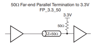
I also tried to connect a termination resistor of 50 ohm pulled up to 3.3 V as recommended for FP_3.3_50 [OFF chip termination]. but it gives nothing...can anyone help me in this?
Hi, I am experimenting with differential outputs on the Arty A7. For this, I am using the 100MHz clock and have instantiated an ODDR then OBUFDS -- . I Have also looked through the 7-series Select-IO Resources User Guide and the only differential I/O at 3.3V is TMDS_33 IOStandard.
Code Verilog - [expand]
The .xdc file has the following --
## Pmod Header JB
set_property -dict { PACKAGE_PIN E15 IOSTANDARD TMDS_33 } [get_ports { buff_out_p }];
set_property -dict { PACKAGE_PIN E16 IOSTANDARD TMDS_33 } [get_ports { buff_out_n }];
Pins E15/E16 are HR I/O banks [JB1/2] and they should work fine.
Synthesis & implementation are fine and I can generate a bitstream, but I see no output on these pins (just 0v)
I also tried to connect a termination resistor of 50 ohm pulled up to 3.3 V as recommended for FP_3.3_50 [OFF chip termination]. but it gives nothing...can anyone help me in this?
Attachments
Last edited by a moderator: