Continue to Site

Welcome to EDAboard.com

Welcome to our site! EDAboard.com is an international Electronics Discussion Forum focused on EDA software, circuits, schematics, books, theory, papers, asic, pld, 8051, DSP, Network, RF, Analog Design, PCB, Service Manuals... and a whole lot more! To participate you need to register. Registration is free. Click here to register now.

difference between Vgg and Vgs

Status
Not open for further replies.

mohamis288

Full Member level 3
Joined
Mar 1, 2022
Messages
165
Helped
0
Reputation
0
Reaction score
1
Trophy points
18
Activity points
1,232
Hi,
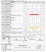
what is the difference between VGG(Q) and VGS? please pay attention to the following datasheet. as you can see, this is a 2-stage power amplifier. please note the page 3 of the datasheet (I have uploaded its picture, as well.) as you can see, VGG(Q) for the first stage is typically 7 volts whereas that one for the second stage is typically 2.7 vols. I have downloaded the large-signal model and as per simulation in ADS, approximately using the same voltage for VGG1(Q) and VGG2(Q) (about 2.4 volts), I have obtained the expected power gain, 32dB. so what is INCORRECT? I apply voltage to the gate of both stage NOT to the gate-source. what is the difference between VGG(Q) and VGS? as per simulation, isn't it correct to write VGS instead of VGG(Q) ?
 

Attachments

  • AFIC10275N.pdf
    1.1 MB · Views: 154
  • page 3.png
    page 3.png
    195 KB · Views: 141

Vgs is the gate-souce difference for a MOSFET (or some
numner of, in parallel.

Vgg would be a single ended supply, ground referred.
-If- all FETs' sources are attached to ground then
"Vgs" and "Vgg" might be the same electrically, but
clarity-of-purpose prefers Vgg as a supply net name.

Maybe some Vgg supplies are noncritical and don't
need to be -exactly- the "typical" value. But for PAE
you wouldn't want any more voltage on the final, than
it takes to accommodate signal swing (& interests such
as clipping / distortion / IP3).
Hi,
Even a small change ( 0.1 volts) in gate voltage, can have a huge impact on drain current. The difference between gate voltage obtained by simulation and
That one written in data sheet is about 4.6 volts ( 7 - 2.4 = 4.6). That is so much!
 

Hi,

Hate to ask, but are you sure your sim circuit is correct as per device requirements, etc.?

I assume you are doing something professional (enough) to contact and query the manufacturer about specific aspects of the simulation model you are using.

I especially like MOSFET models that show e.g. lower RDS(on) than page one, top-right-hand corner specmanship of datasheet could dream of fibbing about, or the models that are equally idealized and ultra-performers but can only be simulated at 27°C... So pinch of salt with anomolies and good to subtract 10% to 20% ideality from the optimistic sim results wrt reality. Or simming circuit conditions that definitely cannot occur in reality (transistors at 20W PD at +150°C Tamb, or resistors capable of the same improbable PD well over 100°C - 'though datasheet PD graph shows 0.0W PD at +150°C).

Anyway, I'd contact the manufacturer to query how to assess the vgg discrepancy between datasheet and your simulation.

If it's too good to believe... you know the rest.

And I'm grateful for post #2 definition of vgg, btw, thanks.
 
Status
Not open for further replies.

Part and Inventory Search

Welcome to EDABoard.com

Sponsor

Back
Top