Continue to Site

Welcome to EDAboard.com

Welcome to our site! EDAboard.com is an international Electronics Discussion Forum focused on EDA software, circuits, schematics, books, theory, papers, asic, pld, 8051, DSP, Network, RF, Analog Design, PCB, Service Manuals... and a whole lot more! To participate you need to register. Registration is free. Click here to register now.

designing switching supply, variable 15-0-15, fixed +5V +3.3V

Status
Not open for further replies.

T3STY

Full Member level 4
Joined
Apr 17, 2012
Messages
239
Helped
24
Reputation
48
Reaction score
24
Trophy points
1,308
Activity points
3,715
Hello everyone! It's good to be back after a long time :)

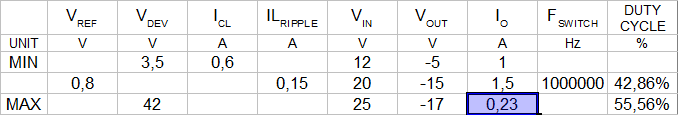
I need to design a nice switching power supply that will be used to power my electronic projects. I need a variable 15-0-15 dual voltage with per-line regulation (for example I want to be able to set -4V and +13V), and two fixed voltages of +5V and +3.3V (the 3.3V might be easily achievable from the +5V line). All lines should draw 1A current, but if it's possible to have more, say 2A, it would be nice yet not necessary.
I have studied** how switching power supplies work, the different topologies and design pros and cons, but I still don't think I'm able to proceed on my own on this task.

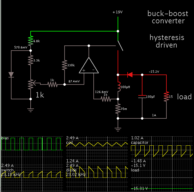
The starting power supply would be a notebook power supply with +19V 4A. Then I was thinking to use some LM2576 (and similar) switching ICs in flyback mode for the -15V supply, and in boost mode for the +15V and +5V supplies. The 3.3V line could be achieved with a 3.3V zener diode on the 5V line, but if you have any better suggestions they're welcome. Datasheet schematics are quite nice for fixed voltages but I don't know how to modify them for variable voltage output. Also, if possible, I would like to include some simple short circuit protection, just in case, but I haven't made any research on that yet.

Can you please help me with this?

** in particular **broken link removed** was the most useful I have found; it is in italian but you might understand the topics from the graphs.
 

Hi,

The 19V input is a good way..
Because of power dissipation i tend to use switching regulators. Step down for 5V and 3.3V.
Also a stepdown for 0..15V. Here you can maipulate the feedback path of the smps to get your desired voltage range.

Also there are inverting topologies. With that and a manipulated feedback you should be able to getc 0..-15V.

Many manufacturers: Lt, maxim, st, ti and many others.

Good luck
Klaus
 

Forget the "zener" option , no good for your application. As mentioned above , use switchers for all 4 outputs.
Might have to put some filtering between the inputs of all the switchers.
Neddie
 

Thanks for the heads up on that zener diode approach. Note taken, use an IC for that as well.

After many searches I found the *LT1074* to be the best IC for all the voltages I need. it can be configured in both buck and inverting topologies, and the good thing is the inverting topology still allows for high current as opposed to many other ICs that could only go up to 900 mA. On page 13 you can find the typical application circuits, and in the pages before there is how to calculate the values for the components.

Next there are the questions of things still unclear to me. I apologize for the numberless questions and for any dumb question.
1) there is an optional filter in the positive-to-negative inverter which uses a 5uH inductor: is that a copper wire inductor or a high-frequency resistor-like component?
2) same question as before for L2 in the buck converter circuit. Also, is the L2-C4 circuit performing the same purpose as the optional filter purposed in the positive-to-negative converter?
3) can you please show me some example filter schematics for connecting in parallel these circuits? if you can include some "general purpose" values for the components it would be great
4) which switching frequency would you recommend using? Could you describe the pros and cons for using low or high switching frequencies? I suppose a high frequency will create more noise, is that correct?
5) PCB layout: is it OK if put all the ICs on the same PCB or should I put each circuit on a separate PCB? Would separating them help reduce any noise?
6) still about PCB: would it help reducing noises on the outside if I'd use a copper or aluminum housing around the PCB (like the ones used on WiFi cards), connected to GND? Maybe with a series resistor? I'm asking this question because the power supply distance from the breadboards is going to be quite small and I fear it would create interferences in the breadboarded circuit and in the power supply as well.
7) D1 is reported to be the *Motorola MBR745* 7.5A Schottky diode. Does it have to be this particular one for any reason or another 7.5A Schottky diode will do well?

Thank you for all your patience if you're willing to answer all those questions :)
 

Hi,

Afaik all LT datasheets have sections ror "inductor selection" and "diode selection". There are detailed description on how to choose the right parts.

Also there are pcb considerations.

Pcb: there wiil be no problem to put all the smps on one pcb. I recommend to use a proper power plane, you can split it for the different smps.

Noise will be no problem also, when you follow the instructions in the datasheet.
I think for breadboard applications you don't need extra filters. The switching regulators work pretty good.

Good luck
Klaus
 

Guys, I can't find how to calculate the values for each component from the available datasheet of the LT1074. At first I thought the formulas given there would allow me to calculate each component's value (probably they do) but I have no idea how to proceed...
Can you give me some help on that?
 

Hi,
LT1074 is a good regulator, i've worked with it many times. But there are more modern devices with higher frequency.
Higher frequency means lower inductivity, smaller package, less loss in inductor and easier post filtering.

Calculating values: for the post filter use the given values, all other you have to calculate with the formulas.

Klaus
 

You mean that I simply change the feedback resistors and all the other components will still be fine?

For other ICs with higher switching frequencies, which ones can you suggest? The LT1074 can go up to 1MHz, are you saying I should get even further than that?
 

The coil is the heart of the action. It will carry a waveform whose peak current rises substantially higher than the maximum current you wish to draw from the output.

Therefore the coil should be rated for maybe 2x your intended current draw. If your spec is 1A at each output, then the coil should be rated at least 2A, for (a) inductive saturation and (b) safe current capacity.

Henry values are flexible. Frequency is flexible.

You may even end up deciding which coil to use, upon spotting a bargain on several coils of the same value.
 

That makes sense! Thanks!
I'm going to evaluate more ICs now, maybe I can find some nicer ones, and then I'll look for some good inductors. Hopefully I'll get something practical done in a week or two ;)
 

Hi,

LT1074 frequency is 100kHz.

If size matters then use a switcher with higher frequency.

To adjust the output voltage there are several ways.
One is to calculate the feedback resistors for the lowest voltage you need an connect an additional variable current source from feedback pin to gnd. Because a current source can be seen as high impedance it does not change stability of the switcher but changes output voltage.

Hope this helps
Klaus
 

Increasing frequency certainly helps with smaller components.
Your switching losses will however increase and so will your inductor core loss.
It also may be harder to pass certain EMI specs. I don't think there is any quick fix here :0)
Build it and see....
Neddie
 

What about using the TI TPS54240 ? 100kHz to 2.5MHz switching frequency seems to be quite a nice range. The price is very low and operating voltage and current ranges seem right for my application.
I would use these regulators at 1 MHz s.f. I have read some notes on various schematics and other datasheets and seems like the 1MHz value is the right one for the best size vs ripple (and side-effects) compromise. Also, I would need some real advice on that because I'll be using this power supply with PICs and other ripple and EMI sensible devices, the last thing I want is to see prototypes going crazy...

EDIT
By the way, thank you all for your previous suggestions ;)
 

I am trying to calculate some parameters using the inverting power supply application note datasheet. When I get to calculate the maximum current the regulator can output it gives the disappointing result of 0.23A. Have a look at the equation 5 of the datasheet linked before:

Io_max <= (ICL_min - (IL_ripple/2))*(1-D_max)

And these are my parameters:
5683844400_1400888243.png

(Io_min = 1A and Io=1.5A are manually set, not calculated)

As you can see the current value is not even near the 1A I am looking for... is it this configuration can't support high current values?
I can't find the ICL_min on the datasheet of TPS54240, and I just set it to 0.6A as in the example. Is this value wrong? I tried putting some random values and only if I set ICL_min=3A I get 1.17A output current...
 

Hi,

I just tried LT's interactive selection guide and feed it with your parameters.
It seems that a switch current of about 3A is needed.

Now i try to calculate it on my own.
19V in, 15V out.
With 19V you "charge" the inductor. With 15V you "discharge" the inductor. Because you charge it with a higher voltage you need less time than to discharge it. The charge time is about 15/ (15+19) = 0.44 = 44%, that is the duty cycle that i expect at full load.
At the output side there is 0.56 = 56% conductivity with a desired average current of 1A. This means 1A/0.56 = 1.78A during conductivity. During this "discharge" time the current varies. This is called the ripple current. The ripple current depends on inductivity. The more Henry, the less ripple current.
Lets assume the p-p ripple current of 1A. With a switching frequency of 1MHz and 56% conductivity it gives a time of 560ns.
L = U × t / I, in values: 15V × 560ns / 1A = 8.4uH.
The current varies from 1.78A - 0.5A = 1.28A to .....2.28A

These are the theoretical values with ideal parts. The reality is worse.
So you may need a switch current of 3A or more and an inductor with 10uH or more.
Mind that the 10uH should be at rated switch current, the inductivity must not saturate.
******
A little more compex than with linear regulators... but no rocket science also.

Hope this helps
Klaus
 

Here is my simulation of a buck-boost converter. It pretty much confirms figures in KlausST's post #15.

Power source 19V.
Output -15V at 1A.


As you can see, your 19V supply must provide well over 2A peak.
So my previous post (#9) gave too low an estimate.
 

Wow! While I never knew all those calculations were required I got gladly lost in all your going through the math! Thank you!

Now, can you please tell me where to look for the switch current value? in the datasheet there is a feature about current limiting through a resistor on the RT/CK pin. Supposing I set this resistor for a 3.2A limit (the power supply says 3.42A, but let's stay 0.22A cooler), will that be the switch current I should consider in the equation?
 

Hi,

As far as i can see in the datasheet you can not set a current limit. It is set to about 6A.
Look for an inductor that can handle this current.
As for your supply, it does not need to supply 6A or 3.2A.The theoretical maximum for the supply current is:
( with L=10uH, Vin= 19V, Ilim=6A, dc =44%, f=1MHz)
ton =44%/1MHz=440ns,
Delta I = U × t / L = 19 V × 440 ns / 10 uH = 0.84A
Imax = 6A, Imin = 6A - 0.84 = 5.16A,
Iavg during on =(6A + 5.16A) /2 = 5.58A
Iavg forcsupply 5.58A × 44% = 2.45A
This is the max avg current that i expect for the 19V supply.

Hope that helps.
Klaus
 

You're right about the current limit, that was for the example IC, TPS54060A. However, the TPS54240 implements an overcurrent protection which slows down the clock speed and basically acts as a current limiter.
I am now making little steps of progress with calculations and seems it goes on well. If nothing will hold me back, next time I post I'll let you know all the values that I have calculated and the circuit and I'll wait for your OK on it ;)
 

I was really hoping to get this done on my own from that point on, but I'm unable to... guys, could someone please do the calculations for me following the inverting power supply application note sheet with a little explaining? At every step in that sheet I find variables and data that I have no idea how to find/calculate, like Vfd, Rdc, Rhs and others. I have also made a spreadsheet (Libre Office .ods file) to avoid actually making all the calculations, I'll attach it to this post if you wish to use it.
 

Attachments

  • Inverting power supply.zip
    30.5 KB · Views: 156

Status
Not open for further replies.

Similar threads

Part and Inventory Search

Welcome to EDABoard.com

Sponsor

Back
Top