Shirai
Newbie
I have a project that is due next week and we need to design an X band amplifier for a gain > 12 dB , NF < 1.5 dB and VSWR < 2.5 while having a DC supply voltage < 5 V .
I have tried many transistors in the ADS library and most has lower operation point than the X-band .
After trying a bunch I simulated one of those transistors I tried using the ADS Designguide for FET Sp , NF , stabilty , ect... and replacing the default transistor by my transistor with this circuit and the following results.


I picked my GammaS and the corresponding Bias point such that I am in the stable region and now , at the input I need to match 50 ohms to that Zs.
I used the smith chart utility to match gamma S to 50 ohms and built my matching network .

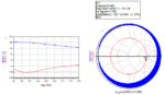
Then when I simulated the circuit with the matching network at the input my S11>-10 dB throughout the frequency range and my gain circle , instead of being the 16.2 dB I got in the designguide simulation for this point ( considering ideal components shouldn't cause losses) I am getting the largest available gain circle implying the lowest possible gain while it is also very thick ( which I don't understand ) .
Also the transistor datasheet didn't have Rn for the NF circle equation so I put it as 5 ohms just to test.

why didn't the matching network work ? and what is the real true gain of my amplifier ?
PS : I tried the tuning tool in ADS and changed the value of the inductance in my LC matching network which gave me better results ( still i don't know why ) but the same issue with my Ga circle . ( should I even use Ga to asses my gain ? I just used it because I was in the GammaS plane so it made sense ) .

Finally these are other results I have if this helps which I don't really understand ( like the shape of the GS circle even if it is in the load plane or my gamma or the fact that my VSWR is within criteria from 9 to 11 GHZ ...)

Please help me , my deadline is super close and I have to write a report and a presentation as well for Wednesday , thursday at most.
Thank you in advance .
I have tried many transistors in the ADS library and most has lower operation point than the X-band .
After trying a bunch I simulated one of those transistors I tried using the ADS Designguide for FET Sp , NF , stabilty , ect... and replacing the default transistor by my transistor with this circuit and the following results.
I picked my GammaS and the corresponding Bias point such that I am in the stable region and now , at the input I need to match 50 ohms to that Zs.
I used the smith chart utility to match gamma S to 50 ohms and built my matching network .
Then when I simulated the circuit with the matching network at the input my S11>-10 dB throughout the frequency range and my gain circle , instead of being the 16.2 dB I got in the designguide simulation for this point ( considering ideal components shouldn't cause losses) I am getting the largest available gain circle implying the lowest possible gain while it is also very thick ( which I don't understand ) .
Also the transistor datasheet didn't have Rn for the NF circle equation so I put it as 5 ohms just to test.
why didn't the matching network work ? and what is the real true gain of my amplifier ?
PS : I tried the tuning tool in ADS and changed the value of the inductance in my LC matching network which gave me better results ( still i don't know why ) but the same issue with my Ga circle . ( should I even use Ga to asses my gain ? I just used it because I was in the GammaS plane so it made sense ) .
Finally these are other results I have if this helps which I don't really understand ( like the shape of the GS circle even if it is in the load plane or my gamma or the fact that my VSWR is within criteria from 9 to 11 GHZ ...)
Please help me , my deadline is super close and I have to write a report and a presentation as well for Wednesday , thursday at most.
Thank you in advance .
Attachments
Last edited by a moderator: