Continue to Site

Welcome to EDAboard.com

Welcome to our site! EDAboard.com is an international Electronics Discussion Forum focused on EDA software, circuits, schematics, books, theory, papers, asic, pld, 8051, DSP, Network, RF, Analog Design, PCB, Service Manuals... and a whole lot more! To participate you need to register. Registration is free. Click here to register now.

Designing a 6V DC to 12V DC converter

Status
Not open for further replies.
Re: DC to DC converter

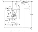
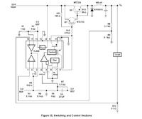
Recently just reviewed the TL494 app note & tried to construct the given example. Couldn't get the original PNP & NPN transistor so I replaced with BD911 & BD912 respectively. My current inductor are about 60uH, output cap is 100V 220uF x 2, setting output voltage to 7.2V ( for my DC powered hand drill which rated 10A@7.2V ).

Others component are similar to SLVA001D app note, but I get about 1v drops on 6A loading. was this normal???
My input are 24VDC.

Also, the sensing resistor are on the GND side, how can I move to Vout for over current protection???
1107551000_1355371933_thumb.jpg


Thanks in advance!
 

In the example the load voltage drops with 0.6V for 6 amp load because of the limiting resistor. Why do you want to move R11 , you need a common ground for something? If the voltage drop bothers you try to use this example https://www.onsemi.com/pub_link/Collateral/TL494-D.PDF for the over current protection that moved tl494 ground on the load ground.
 

In the example the load voltage drops with 0.6V for 6 amp load because of the limiting resistor. Why do you want to move R11 , you need a common ground for something? If the voltage drop bothers you try to use this example https://www.onsemi.com/pub_link/Collateral/TL494-D.PDF for the over current protection that moved tl494 ground on the load ground.

Hello mdorian,

Thanks for yr reply.
I do need a common ground, that's why I'm asking this.
So the voltage drops is normal rite?

Will it possible to have 2 of the circuit I built in parallel to gain more current??
Also, the output=input voltage if the NPN transistor blown/shorted. Any idea how to prevent this???

Thanks!
 

I do need a common ground, that's why I'm asking this.
So the voltage drops is normal rite?
If you review the circuits provided in the discussion thoroughly, you'll notice that there are also TL494 applications with high side current sense. Your schematic from post #41 isn't readable by the way, it's a miniature without real picture.

Shunt voltage drop is a matter of sense amplifier gain and acceptable offset error. You can design a current sense circuit for considerably lower voltage drop. In some cases, a precision amplifier may be necessary. You may want to review the large offer of high side current sense amplifiers from various manufacturers.

Will it possible to have 2 of the circuit I built in parallel to gain more current??
Doesn't sound reasonable. Why not using one controller with more or stronger output transistors?
Also, the output=input voltage if the NPN transistor blown/shorted. Any idea how to prevent this???
Several options;
- Safe design keeping the transistor SOA figures to prevent "blown" transistors
- As ultimate solution a thyristor crow-bar circuit at the output in combination with an input fuse
 

The example schematic are taken from tl494 app note(slva001e).
 

My Copper Wire size of the inductor is 1mm. Was this sufficient for 10A load?
If not how to determine wire size for the desired ampere?

Thanks!
 

Here are the design example from TL494 app note.Thanks!
 

Attachments

  • TL494 design example.jpg
    TL494 design example.jpg
    57 KB · Views: 74

Here are the design example from TL494 app note.
Yes. As said, other design examples mentioned in this thread implement a high-side shunt.

Regarding 10 A with 1 mm wire. This means 12.7 A/mm², not so good. The feasiable current density depends on the core type. As a first step, you may want to put wire length into the calculations and determine the DC resistance and copper losses. You'll find detailed suggestion about wire current density in manufacturer application notes an text books. The Ferrite software from Epcos is a versatile tool for inductor and transformer design.
 

Yes. As said, other design examples mentioned in this thread implement a high-side shunt.
The schematic was uploaded by me previously. But I couldnt understand how it works.
I did some comparison on the 2 schematic & noticed that the current sensing resistor divider was reversed in value.
Regarding 10 A with 1 mm wire. This means 12.7 A/mm², not so good. The feasiable current density depends on the core type. As a first step, you may want to put wire length into the calculations and determine the DC resistance and copper losses. You'll find detailed suggestion about wire current density in manufacturer application notes an text books. The Ferrite software from Epcos is a versatile tool for inductor and transformer design.
I wind the inductor myself with yellow white toroidal ring, will search around Epcos & Google some more info.
 

You can use any discrete or integrated boost converter. However, if you don't need too much power,
simple analog diode voltage doubler can be suficcient:
**broken link removed**

**broken link removed**
 

Status
Not open for further replies.

Part and Inventory Search

Welcome to EDABoard.com

Sponsor

Back
Top