Continue to Site

Welcome to EDAboard.com

Welcome to our site! EDAboard.com is an international Electronics Discussion Forum focused on EDA software, circuits, schematics, books, theory, papers, asic, pld, 8051, DSP, Network, RF, Analog Design, PCB, Service Manuals... and a whole lot more! To participate you need to register. Registration is free. Click here to register now.

Designing a 6V DC to 12V DC converter

Status
Not open for further replies.
Re: DC to DC converter

I don't have much time to study the theory of TL494 driven power supply but at a quick glance it seems that the 0.1 ohm resistors are reading the current for overload protection. Put three additional resistors in parallel and this must solve your problem. This is just a guess so please don't blame me if you burn something.
 

Re: DC to DC converter

Yes, I missed out a connection from C1 & C2 to the collector of Q3 in the schematic.
There are apparently more errors in the present circuit. I e.g. can't detect a path to turn on the output transistor. You may want to show the original circuit source to make us understand what happened to it.

When up-scaling the circuit to 5A, current and power rating of output transistor and diode, inductor current rating, current sense resistors, as already discussed, are affected.

P.S.: BYV32 and IRF9530 are basically suited for 5A output current, but you have to provide sufficient heatsinks for both devices. I think, that a schottky diode would be better, due to both, lower forward voltage and reverse recovery losses.
 
Last edited:

Re: DC to DC converter

I don't have much time to study the theory of TL494 driven power supply but at a quick glance it seems that the 0.1 ohm resistors are reading the current for overload protection. Put three additional resistors in parallel and this must solve your problem. This is just a guess so please don't blame me if you burn something.

Hello mdorian,

I put 4x0.1R now the circuit work very well with 3A load. Thanks!
 

Re: DC to DC converter

Hello mdorian,

I put 4x0.1R now the circuit work very well with 3A load. Thanks!

Take FvM's cautions to prevent overheating and you can try 7X0.1R to raise the overload protection limit to 5A
 

Re: DC to DC converter

There are apparently more errors in the present circuit. I e.g. can't detect a path to turn on the output transistor. You may want to show the original circuit source to make us understand what happened to it.

When up-scaling the circuit to 5A, current and power rating of output transistor and diode, inductor current rating, current sense resistors, as already discussed, are affected.

P.S.: BYV32 and IRF9530 are basically suited for 5A output current, but you have to provide sufficient heatsinks for both devices. I think, that a schottky diode would be better, due to both, lower forward voltage and reverse recovery losses.

Hello FvM, Thanks for yr input.
The P-fet I use is FQP27P06 -> 27A, 60V. mounted on a medium heat sink.
I'll try to replace BYV32 with schottky diode & compare the result.

The original circuit I posted in my 1st post which I missed out a connection from C1 & C2 of TL494 to the collector of Q3.
 

Re: DC to DC converter

The original circuit I posted in my 1st post which I missed out a connection from C1 & C2 of TL494 to the collector of Q3.
Yes, you mentioned this before. But I don't understand how the FET can be driven using exactly this circuit. However, if it's working, you don't need to worry
 

Re: DC to DC converter

Hello FvM,

I also don't understand. But it works.

The original circuit was a 20A, 24v to 12v converter which have 5 pair of the circuit with individual SMD board & heat sink which mounted on a large mother board.

So I asume 1 pair will work at 4A. So am trying to make my self a 5A output with through hole components. I was unable to do so until mdorain pointing out the R10 is 0.1ohm in SMD.

So, 0.1ohm/4 ->0.025ohm right? Will a single 3W 0.025ohm working too? As putting 4 x 5W 0.1R wasting my circuit space.
Will try it when I received the resistor.

About the BYV32, the original SMD was a D-Pak schottky diode 6CWQ06FN, I just notice BYV32 was not a schottky diode after yr advise. Thank you very much. Will try MBR1060CT 10A 60V schottky diode.

---------- Post added at 15:49 ---------- Previous post was at 15:44 ----------

Take FvM's cautions to prevent overheating and you can try 7X0.1R to raise the overload protection limit to 5A

Hello mdorian,

7x0.1R will eat up my circuit space which I'll like to as compact as possible. Am thinking of going lower resistance.
I tried load 4A with 4x0.1R for about 1min it work just find. But I guess this will get very hot on the FET if loading 4A continuously.
 

Re: DC to DC converter

I also don't understand. But it works.
Hm. I also noticed, that the transitor losses aren't optimal yet, so it may be advisable to check the gate voltage waveform and possibly take a closer look at the driver circuit.

Regarding current sense resistors, I would select them mainly for acceptable voltage drop respectively power dissipation, the gain can be changed by a resistor if necessary. Of course you can get single low ohmic shunt devices.
 

Re: DC to DC converter

OK. I just ordered few 3W 0.025ohm resistor will post the result after trying.

Thanks guys for all yr help.
 

Re: DC to DC converter

charge pump is a good choice
 

Re: DC to DC converter

Hello guys,

Now my circuit works very well with 5A load.
24V side 2.6A, 12V side 5A.(drops to 11.6V actually).

But the FET & Schottky Diode is hot, I only can touch the heat sink with my finger for only 1sec, & the IC are in high temp.

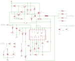
Pls see attached latest schematic. The circuit has some error on the transistor side in my previous schematic.

Thanks!
 

Attachments

  • DC Converter.png
    DC Converter.png
    23.4 KB · Views: 88
Last edited:

Re: DC to DC converter

But the FET & Schottky Diode is hot, I only can touch the heat sink with my finger for only 1sec.
Some losses are normal operation. I suggest to determine the efficiency, by measuring input and output voltage and current, and decide if it's acceptable.
The circuit has some error on the transistor side in my previous schematic.
The gate drive circuit still doesn't look reaonable to me.
 
Re: DC to DC converter

Fvm is right , the current goes only one way because there are only two branches, thru D3 diode and Q2 emitter. At some point the gate will load so much that the current will go back form emitter to base in Q2. Check the schematic again.
 

Re: DC to DC converter

Some losses are normal operation. I suggest to determine the efficiency, by measuring input and output voltage and current, and decide if it's acceptable.
As I mentioned above my input & out are "input 27V(not 24V) ->2.6A, 12.7V ->5A.(drops to 11.6V actually)."
Does this what u mean input & output voltage & current?

Thanks!
 

Re: DC to DC converter

my input & out are "input 27V(not 24V) ->2.6A, 12.7V ->5A.(drops to 11.6V actually)
So the efficiency calculates to 82.6%. Not mind-blowing, but acceptable. A National Simple Switcher IC (LM2679) is said however to achieve about 92% at similar conditions.
 

Re: DC to DC converter

Hello FvM,

Thanks for yr efficiency calculation.
Now my concern are on the heat as the circuit are working very well.
I'll try to load 5A for few hours & see whats going on.
 

Re: DC to DC converter

Someone should please help me with overcurrent protection circuit,overload protection circuit and automatic (loadp) transfer system.
 

Status
Not open for further replies.

Part and Inventory Search

Welcome to EDABoard.com

Sponsor

Back
Top