massive
Member level 2
- Joined
- Jul 20, 2003
- Messages
- 44
- Helped
- 2
- Reputation
- 4
- Reaction score
- 2
- Trophy points
- 1,288
- Location
- Sofia, Bulgaria
- Activity points
- 417
Hi to All,
I would like to ask if someone could give me some info ( paper, or other design document) about the LDO topology that is attached below.
I have not seen it often in papers or LDO design books, etc.
This topology is simple but effective for LDO desgn, to my opinion.
The schematic that is attaced below is simplified and some transistors are not shown
( like cascodes, etc).
Here it is:
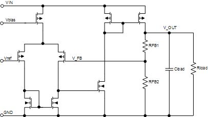
Thanks.
I would like to ask if someone could give me some info ( paper, or other design document) about the LDO topology that is attached below.
I have not seen it often in papers or LDO design books, etc.
This topology is simple but effective for LDO desgn, to my opinion.
The schematic that is attaced below is simplified and some transistors are not shown
( like cascodes, etc).
Here it is:
Thanks.
")