Continue to Site

Welcome to EDAboard.com

Welcome to our site! EDAboard.com is an international Electronics Discussion Forum focused on EDA software, circuits, schematics, books, theory, papers, asic, pld, 8051, DSP, Network, RF, Analog Design, PCB, Service Manuals... and a whole lot more! To participate you need to register. Registration is free. Click here to register now.

Design of microstrip lowpass filter

okik

Newbie level 6
Joined
Oct 18, 2023
Messages
14
Helped
1
Reputation
2
Reaction score
0
Trophy points
1
Activity points
130
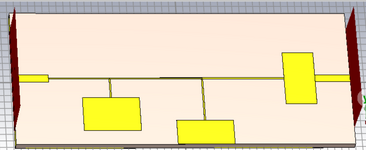
So i have given circuit (link below) and my question is:
Is possible to somehow transform that LC part (L1-Cp1) of that given circuit into microstrip?

1697630193686.png
 
Last edited by a moderator:
Each LC in || has a magnitude of impedance that is equal but opposite phase at the resonant frequency. Thus the length of the 1/4 wavelength controls frequency and the width/depth ratio on gnd. plane controls impedance.

This is for HPF but shows all the variables for different common filters too.
 
Each LC in || has a magnitude of impedance that is equal but opposite phase at the resonant frequency. Thus the length of the 1/4 wavelength controls frequency and the width/depth ratio on gnd. plane controls impedance.

This is for HPF but shows all the variables for different common filters too.
Is this only way how to do it? I mean, i knew values of L=20nH, Cp=1.9pF, Cs=1.2pF, Z=75 ohm - from that can be calculated impedance and not from table as was shown in the video.
 
Do you have a specific tolerance or transfer function for this "almost" Inverse Chebychev 5-pole 1 GHz LPF?

The microstrip will be recursive, unlike fixed lumped elements so is not a good fit in the bandstop region.
 
Last edited:
you are using the WRONG TOPOLOGY for a microstrip Lowpass Filter!

View attachment 186401
THIS will be much easier way to realize an elliptical function lowpass filter
Every lumped strip has an impedance of sqrt(L/C) with resistance. Every shunt capacitance has inductance.

So eventually it can start like your schematic with stripline and grow in complexity depending on your L/C ratios and stripline impedance.

For example this;

1700849300421.png
 
i try to make project in CST from given example, but my simulated S-parameters dont equal expected S-parameters and everything looks right(scheme, lengths/widths of microstrip), so what could be wrong(i think potential problem could be somewhere in CST)?

1701120994784.png

1701120873440.png
 

Attachments

  • 1701120826722.png
    1701120826722.png
    59.5 KB · Views: 61
I don't know what substrate did you use in the simulation shown in #9 but I was able to replicate somehow the S11 and S21 plot (a) using Alumina Dk=9.8 with thickness 0.8mm.
 
i try to make project in CST from given example, but my simulated S-parameters dont equal expected S-parameters and everything looks right(scheme, lengths/widths of microstrip), so what could be wrong(i think potential problem could be somewhere in CST)?
Something is totally wrong with your CST model. The filter must have a through path at DC (0dB insertion loss), but your CST model blocks DC. There might be some gap in the layout.

Edit: Looking at your model screenshot I think the open stub is shorted to the simulation boundary, see arrow.

short.png
 
This is how someone like me would approach your design which I know nothing about your "stepped impedance" filter.
It may have something to do with the assumptions. What happens if the stubs are put on alternate sides?
if i put stubs on alternate side that result is still same,
dont know what else should i change
 
Something is totally wrong with your CST model. The filter must have a through path at DC (0dB insertion loss), but your CST model blocks DC. There might be some gap in the layout.

Edit: Looking at your model screenshot I think the open stub is shorted to the simulation boundary, see arrow.

View attachment 186520
how to solve it?
maybe larger substrate is needed to avoid short circuit?
EDIT: open stub shorted to the simulation boundary was the problem as you mention, so then i made substrate larger(to create gap above stub) and it works!
thank you so much for advice
 
Last edited:
Hello everyone, you help me a lot before and I have request for a help again.
I successfully repeated example in chapter 5.1.3 from this book: HONG, Jia-Shen G.; LANCASTER, Michael J. Microstrip filters for RF/microwave applications. You can see that example above in post #9. So I use this example as guide in my own design of microstrip filter. Everything seems to be fine, but one problem occurs. That is what I want to ask you - how to compensate the unwanted reactance and susceptance presented at T-junction? I mean that relation (5.11) is used in book, but i don't understand how to use it correctly to get correct S-parameter results.
Thanks in advance for any help.
 
i try to make project in CST from given example, but my simulated S-parameters dont equal expected S-parameters and everything looks right(scheme, lengths/widths of microstrip), so what could be wrong(i think potential problem could be somewhere in CST)?

View attachment 186510
View attachment 186509
I stay away from such structures, since the aspect ratio is so far off. The poor electrons do not now if it is a transmission line, or a rectangular resonator! And in any event, the fringing capacitances would be a huge factor!

1704460810593.png


It certainly can not be analyzed as a simple Microstrip transmission line open circuited end!

As an academic exercise, you CAN make structures like this, but require a full emag simulation to figure out how they will react. and they probably then show unwanted higher mode artifacts that make the stop band performance spotty
 

LaTeX Commands Quick-Menu:

Similar threads

Part and Inventory Search

Welcome to EDABoard.com

Sponsor

Back
Top