Continue to Site

Welcome to EDAboard.com

Welcome to our site! EDAboard.com is an international Electronics Discussion Forum focused on EDA software, circuits, schematics, books, theory, papers, asic, pld, 8051, DSP, Network, RF, Analog Design, PCB, Service Manuals... and a whole lot more! To participate you need to register. Registration is free. Click here to register now.

Derivation of transfer function, input and output referred noise of the amplifier configuration

Status
Not open for further replies.

cmawuah

Newbie level 6
Joined
Nov 16, 2020
Messages
14
Helped
0
Reputation
0
Reaction score
0
Trophy points
1
Activity points
101
1. Can someone please help me derive the transfer function of this amplifier configuration?
2. And also the input and output referred noise ignoring flicker noise including Rs, Rin, Rf, M1 and Vin
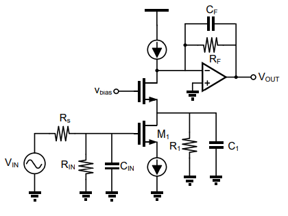
3.PNG
 

1. Can someone please help me derive the transfer function of this amplifier configuration?
2. And also the input and output referred noise ignoring flicker noise including Rs, Rin, Rf, M1 and Vin

View attachment 176551
Why don't you try to do it yourself and then write here where you have difficulties, what your approach is, did you get any results and if you did, why do you think they are not correct. This way you learn much more than looking at some one's derivation. If you want a hint, the transfer function is 0 if you assume the two current sources are perfectly balanced.
 
Why don't you try to do it yourself and then write here where you have difficulties, what your approach is, did you get any results and if you did, why do you think they are not correct. This way you learn much more than looking at some one's derivation. If you want a hint, the transfer function is 0 if you assume the two current sources are perfectly balanced.
@sutapanaki thank you so much for your reply and the hint you have given.

But the problem is, this a try out question that was given to my class for submission on a deadline even though we are yet to get into this topic with our lecturer. This makes it difficult for me and the class to even know how to approach or analyze it in the first place. We've got zero idea on how to do it.

I'll be glad if you could help. Thank you
It wouldn't really benefit you much (especially fellow students) to get the answer for a try out if you have zero idea on how to do it and it's never been taught. I'm guessing he's feeling for how advanced some students might be. Best approach would be to look up Razavi books and gain and noise analysis. I assume that's the book you are using? Have to take it step by step and work up to it.

My first thought is it looks like there is a cascade of two active gain stages.
 
Last edited:

Well, see, you have two ideal current sources - one in the source of M1 and another one as a load. The one that's in the source of M1 provides infinite degeneration, so basically you don't have any gain through the circuit. Transfer is 0. From another point of view, to have a gain you will need to have some AC current flowing through the transistors, but you can't have that because the ideal current source at M1 forces a constant current with no AC.
For the input referred noise in this case - it will be coming only from the input R and C. For example, the noise component from Rs is directly at the input, so no extra work for that. For the noise from Rin, you will have to calculate what noise voltage it creates at the gate of M1 and then refer it back to the input through the voltage divider Rs with Rin||Cin. I think easiest will be for this second component if you take the noise current for Rin, calculate what noise voltage it creates at the gate of M1 (that is the noise voltage across Rs||Rin||Cin) and then refer it to the input.
For the output noise you only have Rf that will generate it. Looking back into the drain of the cascode device you will see infinite impedance (disregarding any parasitic cap there). In this case if you use the noise current for Rf, it will only flow through Rf||Cf and assuming the inverting input of the opamp is at virtual ground, then the noise voltage across Rf||Cf is directly your output noise.
--- Updated ---

I forgot to say that for the output noise I ignored the effect of R1 and C1. You also didn't mention them in your original post. Strictly speaking they will make the impedance looking at the drain of the cascode device not infinite but with some finite value and part of the Rf noise current will go there. And much more of it will go there at high frequencies when C1 starts shorting R1. This will complicate the calculation and lead to a second order expression. I leave it to you for an exercise.
 
Last edited:

Dont forget your Transfer f() algebra rules, they come in quite handy,
making complex circuits that can exhibit simplification due to loading
and isolation, simple.


Regards, Dana.
 

There is a set of Razavi's youtube videos that someone has uploaded that treats Electronics1 and Electronics2 material.
Is there a rule of thumb that says which topology has the best noise performance?
CG gives the best noise performance, CE gives the best gain performance, but for gain and noise performance combined, the cascode CE, CS gives the best of both. Is this a rule of thumb?
--- Updated ---

There is a set of Razavi's youtube videos that someone has uploaded that treats Electronics1 and Electronics2 material.
Is there a rule of thumb that says which topology has the best noise performance?
CG gives the best noise performance, CE gives the best gain performance, but for gain and noise performance combined, the cascode CE, CS gives the best of both. Is this a rule of thumb?
I mean, cascode CE, CG as shown in the figure above from the initial poster, cmawuah
 
Last edited:

There is a set of Razavi's youtube videos that someone has uploaded that treats Electronics1 and Electronics2 material.
Is there a rule of thumb that says which topology has the best noise performance?
CG gives the best noise performance, CE gives the best gain performance, but for gain and noise performance combined, the cascode CE, CS gives the best of both. Is this a rule of thumb?
--- Updated ---


I mean, cascode CE, CG as shown in the figure above from the initial poster, cmawuah
@fgavin there's no rule of thumb stating that.
 

Status
Not open for further replies.

Part and Inventory Search

Welcome to EDABoard.com

Sponsor

Back
Top