Continue to Site

Welcome to EDAboard.com

Welcome to our site! EDAboard.com is an international Electronics Discussion Forum focused on EDA software, circuits, schematics, books, theory, papers, asic, pld, 8051, DSP, Network, RF, Analog Design, PCB, Service Manuals... and a whole lot more! To participate you need to register. Registration is free. Click here to register now.

degrading the THD at the output of the Transmission gate.

Status
Not open for further replies.

balabrahmachari

Newbie level 5
Joined
Jan 30, 2013
Messages
8
Helped
0
Reputation
0
Reaction score
0
Trophy points
1,281
Activity points
1,336
hi All,

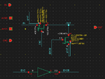
i have made a 8:1 mux (3 selection lines say three stages )using transmission gates as the switches.

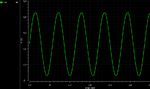
i am getting the THD degraded, at every stage at the switch outputs.

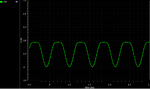
i have observed the input signal is attenuated at the switch outputs.

I am not understand that why the transmission gates wont allow the complete swing of the input?
Can anyone help me please?


thanks in advance...


BALA M..
 

A Cmos CD4066 transmission gate has a non-linear on-resistance of about 100 ohms. If it feeds a signal to a load that has a resistance as low as about 1k ohms or less then the signal level at its output is reduced and the non-linearity shows up on the output. The on-resistance and distortion are less at a higher supply voltage. A CD4051 is a 8:1 mux IC.

If the load resistance is 10k ohms or more then the level is not attenuated and the distortion is much less.

The signal must swing its voltage within the supply voltage of the transmission gate so it must be biased at a voltage that is about half the supply voltage.
 
First suggestions

- describe your setup completely (transistor parameters, supply voltage, signal frequency, load)
- determine the on-resistance versus applied DC voltage level curve for your transmission gate
 
""If the load resistance is 10k ohms or more then the level is not attenuated and the distortion is much less.""

thanks GURU and FvM for your suggestions.

i had put a 10 K ohm load which improved the signal level and THD. but here i had put either M4 or M1 (see in the attachments) will be on at a glance.


but i observed when M4 is on the output is getting clipped. here i am using a 1pf cap load.

when i removed the connection of M4 with the circuit i got THD is -40dB where an the input has the THD around -90dB.

i dont understand why THD is degraded even in the absence of M4. can you help me please?

by the way signal freq is 1.75K, supply voltage 3.3 V, ron i have calculated is 300ohm for M1.
 

Attachments

  • switch.png
    switch.png
    13.1 KB · Views: 89
  • outputclipped.png
    outputclipped.png
    25 KB · Views: 86
  • outputwithout_M4.png
    outputwithout_M4.png
    31.4 KB · Views: 79

Everyone was assuming that you have a standard CMOS transmission gate. It turns out that your transmission gate is NMOS only. So the observed behaviour is expectable.
 

The Cadence schematic is awful to look at since it is a negative image with a black background.
Usually I invert it so it has a normal white background but since it is covered with Chicken Pox dots then I will not bother.
 

Status
Not open for further replies.

Part and Inventory Search

Welcome to EDABoard.com

Sponsor

Back
Top