Welcome to our site! EDAboard.com is an international Electronics Discussion Forum focused on EDA software, circuits, schematics, books, theory, papers, asic, pld, 8051, DSP, Network, RF, Analog Design, PCB, Service Manuals... and a whole lot more! To participate you need to register. Registration is free. Click here to register now.
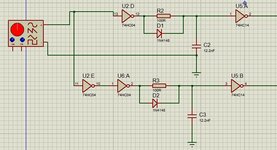
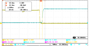
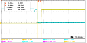
I want to design dead time circuit. I saw dead time circuit in forum. I try it but deadtime is not equal in both side (rising and faling). I added images. How can it is equal deadtime?
To make them identical you need to add a similar delay in the top path to the bottom one so add a buffer ( a non-inverting one! ) before U2D.
However, the question of how the delay is created, it is simply the time constant of R2/C2 and R3/C3 with the diode 'bypassing' the resistor to allow the capacitor to charge faster when the drive signal is high.
I'm not sure what frequency this runs at but the capacitor values seem rather higher than normal.
I assume this is not a production design, given that R-C tolerances, Vth of the gates,
vary all over the map. And multiply those problems by load variation effects you
have a recipe for disaster. Not in the least T and V variations added on top of this
as well.
If you have a processor in design there are families that have accurate stable dead time
control in their PWMs. One example (Uses ~ 12% of chips other resources in just its
fabric area) -
RC dimensioning is far off reasonable values. Consider factor 50 to 100 higher impedance, 5 - 10k, 120 - 240 pF. Presently the assumed undelayed LH transition gets large delay by HC04 output resistance and huge 12 nF capacitor. Actual delay is strongly affected by gate type variations respectively.
First question should be, do you require exactly equal dead times
(follow-ons include "why?" and "to what tolerance"?). How do you
know when you're done?
I have done phase splitters using 3 vs 2 inverters with the "2" having
a simple inverter burden added. Worked "well enough" (but see
quantitative goal setting).
Setting with R and C adds more dimensions to the statistical mix.
Using all MOS might track better.
If you are looking for repeatable nonoverlap on high voltage
swing (like a 40V LDMOS bootstrapped totem pole) then you
have additional problems like how much the common mode
slew time will vary w/ supply, load, temp, process (and, with
drive-limited dV/dt, your nonoverlap time). By this point of
complexity you likely will be looking at adaptive (closed loop
BBM) timing circuit design. Else you will have compound-corner
behaviors rubbing up against either overlap, or bad amounts of
nonoverlap which can mess up the "handoff" between high and
low side switches, possibly overstressing switch elements by
flyback voltage and certainly ruining switching losses by
throwing conduction @ high reverse voltage onto the sync FET
for an interval every period.
a possible solution would be using a D-FF to generate two phase shifted PWM signals (D = 50 %) out of a single input signal. Feed this two signals into two inverters/buffers with TTL compatible schmitt trigger inputs (e.g. 74HCT14). The lower TTL threshold voltages introduces an equal dead time to both of the signals.
The question is what is your aimed duty cycle and dead time? This approach clearly only works for a duty cycle close to 50 %.
Seriously, I don't quite understand what the discussion is about. You are worrying about the additional delay of a single 74HC04 gate (typical 7 ns) which should be related to the intended deadtime of about 1 us according to circuit dimensioning. This is not the problem seen in post #1.
Think about your NOT gate: it has delay, like an RC network, due to input and output resistance and capacitance.
A possible solution: as equal delay is vital to you, read NOT datasheet for logic gate delay and pay attention to shift with temperature, e.g. CD4049 is 200ns to 400ns. Using R x C, select values that at NOT gate definitely ON (1 tau or 3 tau or 5 tau or whatever point in charging curve you need) and place RC network in signal path, i.e. one path = 2 NOTs, other path = RC + NOT . It will not cover full temperature range delay, it is a one-trick pony solution...
e.g. CD4049 = in-to out-delay is 205 to 410 ns
5100 Ohms x 10 pF = 51 ns
51 ns x 5 tau = 255 ns
Presumably a more sophisticated person would make R equivalent to NOT gate output resistance, not just select a random value as I did.
This site uses cookies to help personalise content, tailor your experience and to keep you logged in if you register.
By continuing to use this site, you are consenting to our use of cookies.