Continue to Site

Welcome to EDAboard.com

Welcome to our site! EDAboard.com is an international Electronics Discussion Forum focused on EDA software, circuits, schematics, books, theory, papers, asic, pld, 8051, DSP, Network, RF, Analog Design, PCB, Service Manuals... and a whole lot more! To participate you need to register. Registration is free. Click here to register now.

Darlington based GDT driver

Status
Not open for further replies.
My totem pole is an emitter follower where the Vout is Vin - 1.4 in the case of a darlington transistor
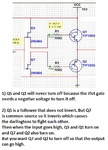
It is about 1.4V when it has no load. The datasheet shows a maximum of 2.5V when it has a load.

I want enough base current to saturate the darlingtons in this situation
Emitter-followers never saturate!
The collector to emitter voltage is never as low as a saturated common-emitter transistor or darlington. So it has the same minimum current gain of 1000 as a linear circuit. The base current is 3mA maximum with a 3A load.
If the emitter is grounded and the load is connected from the collector to the positive supply then it is a common-emitter darlington that needs a base current of maybe 20mA to saturate with a 3A load. The datasheet shows it saturating poorly with a 12mA base current.

But you are saying that the AND cannot supply it without overheating. And even if it could supply the required 12mA, it can't do it at 15V[/quote]
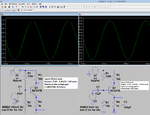
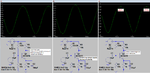
What is the voltage swing and maximum current that you need from this circuit? I saw your load of 2 ohms but saw impossible voltages and many different maximum currents on your simulations.

So then how is it possible to replicate the functionality of a UCC27425, with its Vin and Venable, using logic gates?
The IC is designed to do what you want, why not use it?
 

So using BJTs as a buffer between the logic gates and the darlingtons is not an option because they need too much current and drop too much voltage.

How about JFETs? I have some MPF102s. They have a very small gate capacitance, don't require much current to charge and discharge and are presumably in the range of what the AND gates can supply. And FETs don't drop much voltage compared to BJTs.

I am not really sure how to calculate the required voltage/current to 'open' a MPF102s with a gate capacitance of 7pF it is probably going to be in the order of uA. And from an educated guess from what you have told me thus far, at perhaps 10s or 100s of uA, the AND would probably put out at least 10V which is above the cut off of MPF102

MPF102, and the similar 2N5486, seems to have a maximum drain current of 20mA as far as I can tell from a bit of googling. 0.02A X 15V = 300mW....within the power rating of these devices.

And 20mA would be more than enough to saturate the darlingtons.

Am I doing any better Audio? I am giving this a red hot go and trying to fill in the gaps in my knowledge.

- - - Updated - - -

By the way, I am trying to get QUCS going. I have installed it and it seems easy to use but I can't find any voltage sources in it. I don't know what the hell I have done wrong while installing it. At present I can't create any useful circuits with it. The databse is not very extensive though.

I also have LTSpice but that seems painful to use. I can't see how to rotate components for example.
 
Last edited:

Buffers reduce current, they do not need too much current. But they cause another voltage drop so the output voltage swing will be less. But why bother reducing the very low 3mA darlington maximum base current?
The input junction of a Jfet is always reverse-biased so it ha an extremely low leakage current of 20nA maximum.
The darlingtons are linear emitter-followers that NEVER saturate!

Your new circuit with the useless Jfets has a couple of serious problems:
 

Attachments

  • Jfets and darlingtons.png
    Jfets and darlingtons.png
    109.4 KB · Views: 77

Buffers reduce current, they do not need too much current. But they cause another voltage drop so the output voltage swing will be less. But why bother reducing the very low 3mA darlington maximum base current?
The input junction of a Jfet is always reverse-biased so it ha an extremely low leakage current of 20nA maximum.
The darlingtons are linear emitter-followers that NEVER saturate!

Your new circuit with the useless Jfets has a couple of serious problems:

Are you saying that I don't need anything between the AND gate and the darlingtons or are you saying that the fact that the darlingtons will never saturate is a problem?

Basically what I am ultimately doing is passing a kHz square wave into this circuit and expecting to get a square wave of out of the darlingtons. It has to be fairly high current because it is driving an N30 toroid transformer with one primary and two secondaries. If the current in the primary is too low then the square wave is poorly reproduced in the secondaries.

The induced square wave in the secondaries are what drive the actual power FEts.

- - - Updated - - -

I am assuming that in such a situation the darlingtons need to be acting as switches rather than amplifiers. Perhaps you are suggesting that it does not matter and that I will get my square wave either way.
 
Last edited:

I am assuming that in such a situation the darlingtons need to be acting as switches rather than amplifiers.
They don't necesseraly "need" if you can accept a larger voltage drop, but it's a reasonable objective. Unfortunately none of your circuit ideas is operating the darlington as switch. Consequently you'll restart from the scratch, connecting the darlington transistors in common emitter circuit.
 

With "a kHz" squarewave input, the output of the complementary darlington emitter-followers will be a pretty good squarewave.
The saturation voltage drop of a common-emitter darlington is a little less than the emitter-follower base-emitter voltage drop but the emitter-followers use less base current.
The CD4081 might overheat trying to drive saturating common-emitter darlingtons that have a load current of 3A or more.
 

The inductance of my primary is 1mH and, if I am doing the reactance calculation right, the reactance should be some where around 100 ohms at 20kHz. That is the square wave into the enable pin. But the tesla coil and the signals coming from an aerial and into the in pin might be around 100kHz. Not sure aboutthe total reactance Iin this case. But I doubt that I woild have 3A going through my gdt, perhaps an 1A or so.

Why can't I put a small value resistor on the darlington base to make sure the AND DOESN'T overheat.if it is acting as an amplifier rather than switch anyway.
 
Last edited:

So I will commit this to memory, i.e. that a push pull pair is a form of common collector amplifier.

So the transistors in the push pull pair are operating in their 'active region' as opposed to cut off and saturation, which is why they use less base current. Correct?

A disadvantage must be that, in their active region, the transistors a dropping a larger voltage themselves which means you must be further away from a rail to rail signal when compared to a to a transistor operating in saturation/cutoff. And you need better heat sinking so that the transistors themselves don't overheat. Correct? At least that appears to be what is happening in multisim.

But I can simply make my GDT 1:2:2 or what ever to make up for the lower voltage swing.
 

You should not say "push pull pair" for the linear complementary emitter-followers output because many digital ICs (even the 555 timer IC) have a switching common-emitter push pull output.

To make a transistor or darlington saturate well, it needs a more base current than the current gain calculates for a linear amplifier transistor or darlington. Then the CD4081 might overheat.
When the TIP120 or TIP125 is a linear emitter-follower amplifier, at an output of 3A its maximum base current needs to be only 3mA. But when it saturates in a common-emitter switching circuit its base current must be at least 12mA, and might not saturate very well unless the base current is even higher.
 

With a linear complementary emitter-followers you are using the transistors in their active region where the amplification is at its maximum. Is this correct.

For a load that needs a lot of current what determines whether or not you use a linear emitter-followers or use a transistor as a switch in saturation/cutoff mode?

- - - Updated - - -

With a linear complementary emitter-followers you are using the transistors in their active region where the amplification is at its maximum. Is this correct.

For a load that needs a lot of current what determines whether or not you use a linear emitter-followers or use a transistor as a switch in saturation/cutoff mode?

Actually I think I know the answer to this question now that I think about it.

If you are driving a LED or resistive load then you only need a switch that turns on and off.

But if you are driving an inductive load like a GDT then you need a 'bipolar switch because when you push current into an inductor in one direction and then turn of the switch, the current bounces back in the other direction. If you have a normal transistor switch you then have have a snubber to dissipate the kick back and by doing that you are wasting power.
 

With a linear complementary emitter-followers you are using the transistors in their active region where the amplification is at its maximum. Is this correct?
What is "amplification"? Voltage gain, current gain or both?
An emitter-follower has a voltage gain of 1 like a piece of wire but it has a lot of current gain (low input current but high output current).
A common-emitter transistor usually has a lot of voltage gain and also has plenty of current gain (when it does not saturate) so it can be used as a switch but is difficult to use in a linear push-pull circuit.

For a load that needs a lot of current what determines whether or not you use a linear emitter-followers or use a transistor as a switch in saturation/cutoff mode?
A saturating transistor needs a lot more base current than an emitter-follower then the driver (CD4081) might overheat when it drives saturating transistors.
A 2N3904 little transistor has the same spec's as many other little transistors. As a linear amplifier its current gain is typically 200 but when it saturates its datasheet says to use a base current that is 1/10th its collector current.

(Actually I think I know the answer to this question now that I think about it.)
If you are driving a LED or resistive load then you only need a switch that turns on and off.
But if you are driving an inductive load like a GDT then you need a 'bipolar switch because when you push current into an inductor in one direction and then turn of the switch, the current bounces back in the other direction. If you have a normal transistor switch you then have have a snubber to dissipate the kick back and by doing that you are wasting power.
I think an emitter-follower driving an inductor with a squarewave is allowed only a few volts of "kick back" before its emitter-base junction has avalanche breakdown that slowly destroys the transistor. Even if the collector emitter voltage rating is 100V or more, the avalanche breakdown of the emitter-base occurs at only 5V to 7V. A common-emitter switch does not have this problem.
 

What is "amplification"? Voltage gain, current gain or both?
An emitter-follower has a voltage gain of 1 like a piece of wire but it has a lot of current gain (low input current but high output current).
A common-emitter transistor usually has a lot of voltage gain and also has plenty of current gain (when it does not saturate) so it can be used as a switch but is difficult to use in a linear push-pull circuit.


A saturating transistor needs a lot more base current than an emitter-follower then the driver (CD4081) might overheat when it drives saturating transistors.
A 2N3904 little transistor has the same spec's as many other little transistors. As a linear amplifier its current gain is typically 200 but when it saturates its datasheet says to use a base current that is 1/10th its collector current.


I think an emitter-follower driving an inductor with a squarewave is allowed only a few volts of "kick back" before its emitter-base junction has avalanche breakdown that slowly destroys the transistor. Even if the collector emitter voltage rating is 100V or more, the avalanche breakdown of the emitter-base occurs at only 5V to 7V. A common-emitter switch does not have this problem.

I am thinking of it in terms of the hFE value. When you are using a given transistor in its active region the hFE and current gain is large.

But when you are using it its saturation region the current gain is at its minimum - you use the minimum hFE value when calculating base resistors for a transistor switch.

From the graphs of hFE versus collector current, or what ever, in the datasheets....

With a common emitter amplifier, voltage gain still results from current gain doesn't it?
V = IR and the fundamental functionality of a transistor.

I am thinking of 'amplifier' in terms of an audio amplifier where you have a very tiny audio signal.
 
Last edited:

Can you simply recapitulate what's the intended output voltage and current as well as switching speed of your intended driver? There seems too much confusion in this thread, starting with the title.
 

The hFE is current gain, how much input current is needed to produce a certain output current and affects the amount of voltage gain only a little.
Voltage gain depends on the amount of collector current and the ratio of the collector load resistance divided by the emitter resistor or internal emitter resistance.

For example, with a 10k collector resistor (including the actual load in parallel with it) and a 1k emitter resistor produces a voltage gain of almost 10.
A 10k collector resistor and no emitter resistor or the emitter resistor bypassed with a suitable value capacitor produces a voltage gain of about almost 150.
A 10k collector resistor and a 100 ohm emitter resistor produces a voltage gain of about 80 to 85.
I have never measured the voltage gain when it is high because the distortion will also be high and makes the measurement difficult to see. With low input and output levels the gain can be measured.
Look at my simulations:
 

Attachments

  • transistor gain 1.png
    transistor gain 1.png
    53.1 KB · Views: 69
  • transistor gain 2.png
    transistor gain 2.png
    61.7 KB · Views: 66

OK so the reason why a common emitter configuration requires more base current is due to the collector resistor and emitter resistors which reduces the CE current. To increase the CE current you have to have more BE current.

But you require at least a collector resistor otherwise the output would flat line at Vcc or close to it. With the resistor in place, the input signal draws down the C output voltage from Vcc when it goes positive and opens the CE junction such that some of the voltage is shared with the CE junction as in a voltage divider.

With the complementary pair the transistors are on alternately so the collectors of each or isolated from Vcc or GND by the other. Hence the reason they follow the voltage of the base input -Vbe. With no collector or emitter resistors a much smaller base current results in a big output current.

Am I correct?
 

OK so the reason why a common emitter configuration requires more base current is due to the collector resistor and emitter resistors which reduces the CE current. To increase the CE current you have to have more BE current.
N0. The definition of saturating a transistor is to increase the base current until the base-collector junction conducts current then some of the base current flows into the collector. In an emitter-follower the base collector junction never conducts because it is always reverse-biased.

But you require at least a collector resistor otherwise the output would flat line at Vcc or close to it. With the resistor in place, the input signal draws down the C output voltage from Vcc when it goes positive and opens the CE junction such that some of the voltage is shared with the CE junction as in a voltage divider.
The input signal to a common-emitter transistor causes the transistor to conduct more and less collector-emitter current. This varying collector current flows in the collector resistor and Ohm's Law shows that it produces a varying voltage across it.
With no collector resistor then the transistor simply shorts the power supply.

The emitter resistor in a common-emitter transistor circuit applies some negative feedback due to the collector-emitter current in it reducing the actual base-emitter signal voltage. The emitter resistor also reduces the effect of temperature and the range of base-emitter voltages for different transistors.

With the complementary pair the transistors are on alternately so the collectors of each or isolated from Vcc or GND by the other. Hence the reason they follow the voltage of the base input -Vbe. With no collector or emitter resistors a much smaller base current results in a big output current.

Am I correct?[/QUOTE]
 

I like this description of how a common collector/emitter follower works Audio - this makes immediate sense to me: **broken link removed**

Particularly this bit:

Ve up => Vbe down => Ib down => Ic down => Ve down => Vbe up ...........

So my GDT primary is providing negative feedback to my darlington base - therefore it is impossible to saturate my darlingtons in this configuration.

I am happy with that and I now have a good understanding of what you have been trying to get across to me.

- - - Updated - - -

Aahhhh.

http://www.electronics-tutorials.ws/transistor/tran_4.html

A transistor as a switch is a type of common emitter amplifier, except that there is no voltage divider on the base, only a series resistor to put a limit on the base current.

So the base is either above GND or at or below GND and it is only used with strong input signals. So the transistor is either fully on or fully off. And there is no emitter resistor to provide negative feedback.

I think I have previously been confused by the fact that the load resistor often forms the base resistor another bigger transistor.
 

Status
Not open for further replies.

Part and Inventory Search

Welcome to EDABoard.com

Sponsor

Back
Top