Vsl
Newbie level 3
[CST] How to simulate an ISS ( impedance standard substrate )
Dear all,
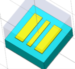
I'm tryng to simulate a CST structure like the one you can see in the picture. The structure represent the Open standard realized with alumina on a silicon substrate.
The three pads represents the landing pads of a typical ground-signal-ground probe.
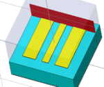
The problem is how to simulate them. Do you suggest to use a waveguide port ( as shown in the second picture ) or three lumped port, one on each pad?
Thank you in advance,
V.M.

