Continue to Site

Welcome to EDAboard.com

Welcome to our site! EDAboard.com is an international Electronics Discussion Forum focused on EDA software, circuits, schematics, books, theory, papers, asic, pld, 8051, DSP, Network, RF, Analog Design, PCB, Service Manuals... and a whole lot more! To participate you need to register. Registration is free. Click here to register now.

Constraints for the Clock Dividers of Double Edge Triggered FFs

Status
Not open for further replies.

ranaya

Advanced Member level 4
Full Member level 1
Joined
Jan 22, 2012
Messages
101
Helped
4
Reputation
8
Reaction score
9
Trophy points
1,298
Location
Kelaniya
Activity points
2,164
Dear All,

I have a design that looks like below. The design first receives a single edge triggered clock and through some clock gates, this clock signal is divided by 2 to convert it to a double edge triggered (DET) signal. The idea here is to incorporate DET FFs in a larger digital design. Since standard CAD tools do not understand DET behaviour, the placement of DETs after the initial synthesis is customly made. So that the timing graphs can be re-generated using DET timing in design compiler.....
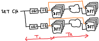
1631172482296.png


How should we specify the sdc constraints for the clock tree at PnR stage ?

Thanks
 

Hi,

I think I don´t understand. Can you please draw a timing diagram.

***
I may be mistaken ..
But isn´t
* "dividing the clock by 2 and then use it double edge triggerd"
the same as
* "non divided clock used as signle edge triggered"?

****
And usually you avoid to divide clocks but just generate a divided "clock_enable" signal.
(at least on FPGAs)

Klaus
@KlausST

Hi, the diagram looks like below :
1631174161745.png


Assuming DET clock load is less than the x2 of the SET clock load (this has been proven in circuit), in this approach, the DET consumes less power than the SET. This is the end-goal I want to achieve ! However as you said, data-throughput-wise, they are both same !
 

Hi,

So it´s because of power consumption.
I´m sorry, I can´t help you with this, I´m not experienced in this field.

Good luck.

Klaus
 
IC design tools had some experimental support for double edged clocks a few years ago. But my understanding is that this trend became less and less popular. I am not sure the support is still there.
 
Status
Not open for further replies.

Part and Inventory Search

Welcome to EDABoard.com

Sponsor

Back
Top