Continue to Site

Welcome to EDAboard.com

Welcome to our site! EDAboard.com is an international Electronics Discussion Forum focused on EDA software, circuits, schematics, books, theory, papers, asic, pld, 8051, DSP, Network, RF, Analog Design, PCB, Service Manuals... and a whole lot more! To participate you need to register. Registration is free. Click here to register now.

[SOLVED] colpitis oscillator and positive feedback

Status
Not open for further replies.

akbarza

Full Member level 2
Joined
Dec 18, 2013
Messages
131
Helped
0
Reputation
0
Reaction score
0
Trophy points
1,296
Activity points
2,556
hi
i tried to uplaod a pic of a circuit three times, but it was paused at 100percent . its address in gdrive is:
https://drive.google.com/file/d/1tQ5g5hVVtu5pZekBOl1jjmScpuK2WKuf/view?usp=sharing
it is only 79.1kB, So if the pic is not here, plz refer to above address.
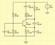
i simulate the circuit in ltspice. the circuit is a colpits oscillator. my questions areabout the circuit:
  1. i know that for oscillation, there must be positive feedback. where is positve feedback?plz,explain
  2. what is roles of c3 and c4 ?
  3. when i saw output and i take fft of it( in ltspice) the total harmonic distortion(THD) was 18.32%. what can be done to the output be more sinosidal wave( namely, better THD)?
  4. when i saw output, it was a wave with amplitude between 0.7v and 18.5v. as you can see in pic the voltage source is 18 volt. is it possible and is ecceptable that the value of output is larger than power supply?
thanks
 

Attachments

  • 1.PNG
    1.PNG
    79.2 KB · Views: 101

C4 ties the Base to GND so it's a Base Grounded Colpitts Oscillator.
L1 Could be connected directly to Power Supply but the designer intends to decrease the damping to stabilise the oscillations by R2. Otherwise C3 is a very big capacitor that makes the inductor to Vcc so GND. L1 is essentially parallel to feedback capacitor pair and defines also oscillation frequency.
Oscillators works almost rail-to-rail. So seeing 0.7V-18V sinusoidal signal is normal (open circuit voltage). But you have to charge this circuit with appropriate load. You will see the difference. It will maybe stop to oscillate.
THD is another concern. It depends on absolutely operating point, driving power, nonlinear components' specifications.
 
Last edited:
This circuit operates by a common base DC voltage modulating the emitter to oscillate in phase with the collector with gain >1. Most of the time Vbe is reverse biased but when Vc drops in phase with Ve, Vbe which becomes forward biased at 0.6V and creates an impulse of Ic current which pulls down Vc and Ve until the C2 coupled voltage decays. This positive feedback creates a high current impulse about 1% of the frequency then for 99% of the time the transistor current is zero.and the LC circuit just rings being much lower impedance than Rc=47k.

The output voltage envelope declines well below Vcc at steady state and the impulse current changes shape but continues to distort the sinewave voltage output for a small portion of the cycle, thus not being a clean ~1 MHz Sine Oscillator. It pings from Vbe to Ic impulses and the positive feedback DC gain of Rc/Re is sufficient to keep it oscillating. ping ping ping.

It needs work to improve, I would suspect to meet the design expectations. What design specs do you have?

1701304742769.png

--- Updated ---

With L on the collector to Vcc, you can expect Vc to rise "towards" double the supply Vcc with ideal oscillations. But damping impedance reduces the envelope size.
 
Last edited:
Without simulating the given circuit, I'd expect strong distortions due to large feedback factor. You can try to play with C1/C2 ratio to tune it. But reducing feedback will result in lower output voltage and increased load sensitivity.
 

This circuit operates by a common base DC voltage modulating the emitter to oscillate in phase with the collector with gain >1. Most of the time Vbe is reverse biased but when Vc drops in phase with Ve, Vbe which becomes forward biased at 0.6V and creates an impulse of Ic current which pulls down Vc and Ve until the C2 coupled voltage decays. This positive feedback creates a high current impulse about 1% of the frequency then for 99% of the time the transistor current is zero.and the LC circuit just rings being much lower impedance than Rc=47k.

The output voltage envelope declines well below Vcc at steady state and the impulse current changes shape but continues to distort the sinewave voltage output for a small portion of the cycle, thus not being a clean ~1 MHz Sine Oscillator. It pings from Vbe to Ic impulses and the positive feedback DC gain of Rc/Re is sufficient to keep it oscillating. ping ping ping.

It needs work to improve, I would suspect to meet the design expectations. What design specs do you have?

View attachment 186558
--- Updated ---

With L on the collector to Vcc, you can expect Vc to rise "towards" double the supply Vcc with ideal oscillations. But damping impedance reduces the envelope size.
hi and thanks for the reply
I read your reply three times. I want to know about the colpits oscillator only and it is not related to any project.
I passed some courses about electronics in university several years ago and I also like electronics so when I find a subject about electronics on the net, I read some about it.
finally, if I want to know more about this subject, which reference (book, site,...) do you suggest to me?
thanks again
--- Updated ---

h
Without simulating the given circuit, I'd expect strong distortions due to large feedback factor. You can try to play with C1/C2 ratio to tune it. But reducing feedback will result in lower output voltage and increased load sensitivity.
i
what is load sensitivity?
is feedback factor value as c1/(c1+c2) which is half in this circuit?
 

I have difficulties to get sine waveform with present circuit. Used more standard colpitts:

1701337545920.png
 

Attachments

  • colpitts1.zip
    783 bytes · Views: 47

  1. i know that for oscillation, there must be positive feedback. where is positve feedback?plz,explain
  2. what is roles of c3 and c4 ?
* It is a common base configuration due to the capacitor C4.;
* The inductor L and the capacitors C1, C2 form a grounded tank circuit with maximum amplitude (and zero phase shift) at the resonant frequency wo.
* A portion of the collector output voltage is coupled back to the emitter. Because the voltage gain between emitter and collector (due to the common base configuration) is positive, we have positive feedback at w=wo.
* The capacitor C3 is needed in the shown circuit because the desired DC operational point is fixed with a collector resistor R2 (not part of the classical Colpitt circuit). Otherwise, the inductor L would be a DC short for R2. The value of C3 must be large enough not to influence the resonant frequency.
 
Last edited:
The Colpitts in OP's post is the type that has the power supply in the resonating loop. This is not necessarily bad although it has current flowing back and forth through the power supply. Various influences (known and unknown) may enter in.

There are other configurations where the LCC tank resonates without any other component in the resonant path. That type may yield a sinewave which is less distorted. Example below. Notice current drawn from the supply is a small fraction of current that builds in the LCC tank.

Colpitts oscillator LCC tank at right 7 MHz.png
 
h
Without simulating the given circuit, I'd expect strong distortions due to large feedback factor. You can try to play with C1/C2 ratio to tune it. But reducing feedback will result in lower output voltage and increased load sensitivity.
i
what is load sensivity?
is feddback factor value as c1/(c1+c2) which is halfin this circuit?
I have difficulties to get sien waveform with present circuit. Used more standard colpitts:

View attachment 186565
hi
as i know, we first do dc analysis. because l1 is connected to vcc, the output( collector of transitor) is biased at vcc and there is not room for output voltage , so it must cause very large distortion.
--- Updated ---

h
Without simulating the given circuit, I'd expect strong distortions due to large feedback factor. You can try to play with C1/C2 ratio to tune it. But reducing feedback will result in lower output voltage and increased load sensitivity.
i
what is load sensivity?
is feddback factor value as c1/(c1+c2) which is halfin this circuit?
I have difficulties to get sien waveform with present circuit. Used more standard colpitts:

View attachment 186565
hi
as i know, we first do dc analysis. because l1 is connected to vcc, the output( collector of transitor) is biased at vcc and there is not room for output voltage , so it must cause very large distortion.
This circuit operates by a common base DC voltage modulating the emitter to oscillate in phase with the collector with gain >1. Most of the time Vbe is reverse biased but when Vc drops in phase with Ve, Vbe which becomes forward biased at 0.6V and creates an impulse of Ic current which pulls down Vc and Ve until the C2 coupled voltage decays. This positive feedback creates a high current impulse about 1% of the frequency then for 99% of the time the transistor current is zero.and the LC circuit just rings being much lower impedance than Rc=47k.

The output voltage envelope declines well below Vcc at steady state and the impulse current changes shape but continues to distort the sinewave voltage output for a small portion of the cycle, thus not being a clean ~1 MHz Sine Oscillator. It pings from Vbe to Ic impulses and the positive feedback DC gain of Rc/Re is sufficient to keep it oscillating. ping ping ping.

It needs work to improve, I would suspect to meet the design expectations. What design specs do you have?

View attachment 186558
--- Updated ---

With L on the collector to Vcc, you can expect Vc to rise "towards" double the supply Vcc with ideal oscillations. But damping impedance reduces the envelope size.
hi
can you introduce a refrence for more information?
 
Last edited:

as i know, we first do dc analysis. because l1 is connected to vcc, the output( collector of transitor) is biased at vcc and there is not room for output voltage , so it must cause very large distortion.
Don't agree with explanation. As shown in post #6, you get good sine waveform with slight circuit modifications (towards a standard colpitts). Problem of original circuit is I think, that 47k resistor and C3 make it difficult to get a stable operation point. Usual colpitts circuit doesn't have it.
 

The Colpitt’s sine quality depends on a high Q factor and an impulse of current every negative cycle peak after reaching bias steady-state (SS). The DC path through L is essential towards achieving low distortion and up to 2x Vcc swing.
Run the simulation for at least 10xQ cycles to reach SS. The two caps offer a course and fine tuning of f with L, because the net C is more sensitive to change from the smaller C-E series capacitor, which also raises the impedance. from sqrt(L/C)=Z

The Clapp oscillator shown by Brad can use either collector output with a low Rc value like 100 ohms or emitter output. This version is preferred for it’s low output impedance, high Q and low distortion.

The origin of the circuit in this question is unknown but certainly not low distortion nor a Colpitt’s design.
 
Last edited:

The Colpitts in OP's post is the type that has the power supply in the resonating loop. This is not necessarily bad although it has current flowing back and forth through the power supply. Various influences (known and unknown) may enter in.

There are other configurations where the LCC tank resonates without any other component in the resonant path. That type may yield a sinewave which is less distorted. Example below. Notice current drawn from the supply is a small fraction of current that builds in the LCC tank.

View attachment 186568
hi
i simulate your circuit in ltspicewith 2n222, 2n3904 bjt, but there is not any oscillation
--- Updated ---

hi BradtheRad
there is no oscillation with the below schematic(i simulated in ltspice):
colpitts5.png
 

We don't know which transistor model is used in post #8. The circuit works for me in LTspice with 2N2904 and inductor increased to e.g. 10 uH. I'd prefer a standard colpitts circuit though, as already stated.
 

Status
Not open for further replies.

Similar threads

Part and Inventory Search

Welcome to EDABoard.com

Sponsor

Back
Top