Welcome to our site! EDAboard.com is an international Electronics Discussion Forum focused on EDA software, circuits, schematics, books, theory, papers, asic, pld, 8051, DSP, Network, RF, Analog Design, PCB, Service Manuals... and a whole lot more! To participate you need to register. Registration is free. Click here to register now.
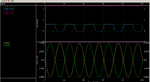
What can be done to avoid clipping on the positive side. Vdd is at 3.3 and VSS is at 0. I am giving an 8mv differential sine wave at the input. The common mode voltage (vref) is 1.5.
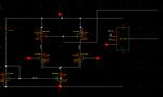
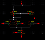
Your negative images were so black and with the parts so far apart that it was difficult to see the text.
So I inverted it to make it a normal positive image then I cropped and enlarged it so it is large enough to read the text.
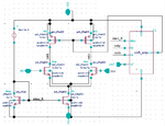
Try making the bottom supply rail a negative polarity whose amplitude is same as your positive supply. Adjust bias values to bring your output waveform down so it's centered on 0V.
Speaking of bias it's usual to build a simpler bias arrangement which has fewer wires running to and fro.
Try making the bottom supply rail a negative polarity whose amplitude is same as your positive supply. Adjust bias values to bring your output waveform down so it's centered on 0V.
Speaking of bias it's usual to build a simpler bias arrangement which has fewer wires running to and fro.
My design requires me to keep the lowest voltage at 0 and highest at 3.3. I want to amplify a small differential signal (common mode at roughly halfway between the supply and the ground) and maintain the same common-mode at the output. The differential signal is getting amplified properly for the negative half but gets clipped at the positive half. what device parameter has to be changed to try and reduce the clipping?
I have checked the operating points. The top PMOS transistors have enough headroom to stay in saturation yet still somehow the waveform is getting clipped.
My design requires me to keep the lowest voltage at 0 and highest at 3.3. I want to amplify a small differential signal (common mode at roughly halfway between the supply and the ground) and maintain the same common-mode at the output
I believe you need to add more DC component to your incoming AC signal. That should shift circuit behavior midway between supply and ground. (The arrangement is similar to a class A amplifier.) As you adjust the signal up or down, you should be able to position the output so the entire waveform is visible with no clipping.
The principle becomes obvious if you experiment with a simple class A amplifier and oscilloscope.
This site uses cookies to help personalise content, tailor your experience and to keep you logged in if you register.
By continuing to use this site, you are consenting to our use of cookies.