Continue to Site

Welcome to EDAboard.com

Welcome to our site! EDAboard.com is an international Electronics Discussion Forum focused on EDA software, circuits, schematics, books, theory, papers, asic, pld, 8051, DSP, Network, RF, Analog Design, PCB, Service Manuals... and a whole lot more! To participate you need to register. Registration is free. Click here to register now.

Charge Pump, Problem with diode

Status
Not open for further replies.
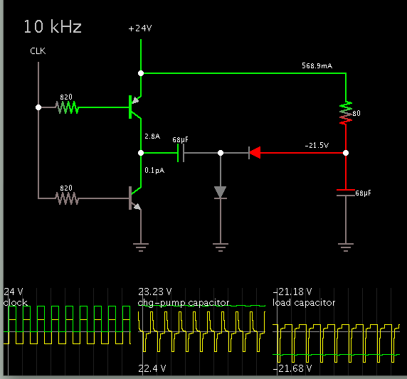
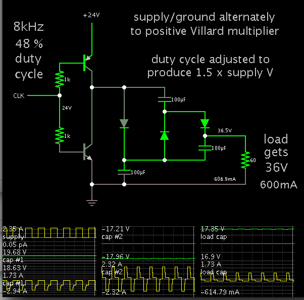
As I considered your simulation, the output is rely on load definitely and whenever the load changes (for example from 80 ohm to 120 ohm), output voltage goes from 38V to 40V. in previous design, we didn't have similar changes to output voltage by variation of load.
 

the output is rely on load definitely and whenever the load changes (for example from 80 ohm to 120 ohm), output voltage goes from 38V to 40V. in previous design, we didn't have similar changes to output voltage by variation of load.
Does it actually change? In this case, if the voltage is critical, you should use a regulator.

I'm not sure about the primary design criteria. Is it part count and size, efficiency, output stability?
 

The load affects output voltage to a greater extent with the mosfets, because they evidently are not biased as much as they could be (in Falstad's simulator, anyway).

With the transistor version, it is easier to drive a heavier load. The base currents can be increased or decreased to match.

Here is my transistor version. It turns out 2 of the transistors are unnecessary. The diodes were necessary at first because NPN's started to permit backflow from the emitter up through the base. With some fiddling it appears the diodes are sufficient to take the place of 2 transistors.


It starts to look like your original charge-pump, doesn't it? (FvM drew a similar comparison).

However with this circuit, the current surges are less since they take up a longer duty cycle.

If the base resistors are too low ohms, it causes current to be wasted as it goes directly out the PNP base, and into the NPN base.

Here is the link which will load the above simulation.

https://tinyurl.com/d9ks4jx
 

@BradtheRad, the main advantage of your current design is power dissipation which is decrease than this one


however your design delivers 45V p-p at output while my latest question was:
I have another question, is there any ways to generate -12V instead of -24V from the positive power supply of +24V? in other word I have totally 36V p-p at output instead of 48V?

As FvM said, maybe using some chips have better result such as MC34063. according to step-up converter topology placed below, maximum output current is 0.175A which is not enough.
furthermore, for driving even small motors, some ICs as supplier with PDIP package is not suitable.


Another IC is LM2576 with TO-220 package and max 3A output. below, you can see Buck-Boost inverter with this chip. if the input voltage be 24V, it delivers -12V. therefore total output voltage is 36Vp-p @ 700mA.
 

the main advantage of your current design is power dissipation which is decrease than this one
Really? How do you determine it?

Buck converter IC in inverting configuration, e.g. LM257x or LM267x, is a solution with acceptable part count and high efficiency. MC34063 would need an external switch transistor for the intended current range, as shown in post #16. Nevertheless it's prefererred in some cases for it's low price.

I just realized, that you also referred to charge pumps with rational voltage ratios (in post #15). That's in fact a principle option. But I don't believe that it applies for a discrete implementation, due to large number of involved switch transistors and their respective gate driver circuits. A few chips of this type are commercially available, but not for currents in the range of interest.
 
Really? How do you determine it?
with falstad simulation ofcourse

The schematic in post #15 was come from this article:
"High-Efficiency, Regulated Charge Pumps for High-Current Applications" By Brigitte Kormann, 2003
in the page #3 of this article, you can see "1.5-times transfer charge pump" topology.
It is perhaps that this topology be the manufacturing technology of some chips and discrete implementation of that not be optimized because of some constraint.
 

@BradtheRad, the main advantage of your current design is power dissipation which is decrease than this one


however your design delivers 45V p-p at output while my latest question was:

I have another question, is there any ways to generate -12V instead of -24V from the positive power supply of +24V? in other word I have totally 36V p-p at output instead of 48V?

I gave the transistors ample bias, so as to demonstrate that the maximum output can go up to 45V for a load in the range of your motor.

However you can decrease the bias current in the transistors, in order to obtain whatever volt level you want at the load. This is creating a voltage drop by creating resistance in the transistors (linear mode). It is inefficient, so maybe you would rather not use that.

In your original schematic you used a 10uF capacitor. As FvM pointed out (post #16), changing this capacitor is one way to raise or lower the final voltage. This is voltage drop via capacitive reactance. The voltage swing on a smaller capacitor is greater, hence it reduces net current flow.

I have been looking over my large collection of voltage multiplier schematics. I thought I had one that produces 1.5X from DC pulses. It might need 2 transistors, or it might need 1 transistor.

I may be able to poke and prod one so that it puts out 600mA at 36V, at an acceptable efficiency level.

- - - Updated - - -

I almost forgot, you can also reduce the duty cycle by reducing transistor 'ON' time. It is not a resistive drop method. It does not reduce efficiency. It will reduce voltage at the load.

There is still the matter of voltage regulation at the load, however.
 

I almost forgot, you can also reduce the duty cycle by reducing transistor 'ON' time. It is not a resistive drop method. It does not reduce efficiency. It will reduce voltage at the load.
I suppose, a thorough simulation will give a different picture. The operation of the charge pump is ruled by charge balance. As a result, for the single stage "voltage doubler" the average current delivered to the load will be equal to the average input current, or lower if cross-conduction happens in the push-pull stage.

Under this prerequisites, the efficiency of the circuit is |Vout/Vin|, equal to a linear regulator. That's obvious because a capacitor can't transform energy between different voltage levels as an inductor does.

You can use capacitors to transform voltages without large losses, if you switch capacitors between parallel and series circuit, keeping the voltage accross the capacitors almost constant. That's the operation principle of the circuit in post #15 and commercial ICs like LM3350.
 

I wrote:

I almost forgot, you can also reduce the duty cycle by reducing transistor 'ON' time. It is not a resistive drop method. It does not reduce efficiency. It will reduce voltage at the load.

I suppose, a thorough simulation will give a different picture.

I should have said...

Given the 70 to 80% efficiency of the charge pump method (stepping 24V up to 36V)...

It does not improve or reduce its efficiency by adjusting the duty cycle to change the output voltage.

I remember that I gave the wrong idea (some months ago here) when I stated a supply voltage can be dropped to a lower, at 90% or better efficiency, by chopping it into pulses onto a capacitor at the desired duty cycle, and smoothing the result. I remember I had to be set right (and you FvM were helpful in that regard).

You can use capacitors to transform voltages without large losses, if you switch capacitors between parallel and series circuit, keeping the voltage accross the capacitors almost constant. That's the operation principle of the circuit in post #15 and commercial ICs like LM3350.

Yes, I have been experimenting with various simulations of switched capacitors because the idea holds promise.

However I find it's a headache figuring out how to replace the switch 'icons' with real transistors/mosfets, in such a way that they work correctly.
 

is there any ways to generate -12V instead of -24V from the positive power supply of +24V? in other word I have totally 36V p-p at output instead of 48V?

I do not seem to find a simple voltage multiplier that increments in units of 0.5 x supply V. This is because the tendency is for capacitors to charge immediately to the supply voltage. As a result, increments are in the amount of whatever is the supply V. If it is a lesser amount, it is due to diode drops and resistive drops.

The best I have come up with is the schematic below. It is a Villard tripler, driven by alternating supply and ground connections. The duty cycle has been adjusted to provide 1.5 x V.

It does not overload the diodes quite as much.

It is not necessarily a big improvement on your original charge-pump schematic in post #1.


There can be several variations on this theme:

The voltage multiplier can be positive or negative depending on how the diodes are oriented.

Power can be taken across the output and ground rail, or across the output and positive rail.

Additional stages can be added as desired.
 

I implemented Buck-Boost inverter topology with LM2576-12 from National manufacturer. I applied +28V input voltage and I could deliver -12V output without any problems. however I didn't see Buck-Boos inverter for LM2576-Adj in datasheet. can I use this topology for LM2576-Adj or not?
 

@BradtheRad, I simulated your design in post #30. in your schematic, desired output will be achieved if power stage consists of BJT transistors and precise value of base resistors.
Assume switching by MOS transistors which deliver 0~24V pulses to multiplier stages. I simulated it by square wave generator and you can review it in the link below. what result I saw in output is still near to 48V.
I guess in practice if I would implement power stage by bjt transistors, because of different characteristics of BJT Transistors, I had wide range of output voltage and also temperature dependency of output. for example replace 1k resistors by 1.1k. you can see output drops 3 Volts and reduces to 33V.

**broken link removed**

also the export link is below:
https://tinyurl.com/bvlrqva
 

I simulated your design in post #30. in your schematic, desired output will be achieved if power stage consists of BJT transistors and precise value of base resistors.
Assume switching by MOS transistors which deliver 0~24V pulses to multiplier stages. I simulated it by square wave generator and you can review it in the link below. what result I saw in output is still near to 48V.
I guess in practice if I would implement power stage by bjt transistors, because of different characteristics of BJT Transistors, I had wide range of output voltage and also temperature dependency of output. for example replace 1k resistors by 1.1k. you can see output drops 3 Volts and reduces to 33V.

Yes, your simulation acts the same way I saw mine.

It requires precise adjusting of transistor bias, to obtain a desired volt level on the load. Even then there can be temperature-related inconsistencies. The Falstad simulator does not model temperature-related behavior.

To get better regulation, it should be possible to provide a feedback signal to the clock generator, so it will adjust its duty cycle automatically. A 555 might even be made to do the job. It might require an op amp in between.

This method (charge-pump with capacitors) seems to need a growing number of components. At some point it becomes practical to consider a switched-coil converter instead.
 

Status
Not open for further replies.

Similar threads

Part and Inventory Search

Welcome to EDABoard.com

Sponsor

Back
Top