Continue to Site

Welcome to EDAboard.com

Welcome to our site! EDAboard.com is an international Electronics Discussion Forum focused on EDA software, circuits, schematics, books, theory, papers, asic, pld, 8051, DSP, Network, RF, Analog Design, PCB, Service Manuals... and a whole lot more! To participate you need to register. Registration is free. Click here to register now.

Bubba Oscillator and THD

Status
Not open for further replies.
I forgot to enclose the pdf-file.
 

Attachments

  • RDS.pdf
    59.1 KB · Views: 70

I have never seen a SK104 or SK105 datasheet. A summarized specification says:
2SK104
N-Channel JFET
Various
field effect transistors,transistors
V(BR)GSS (V)=30
I(D) Abs. Drain Current (A)=20m
I(G) Max. (A)=10m
Absolute Max. Power Diss. (W)=250m
I(GSS) Max. (A)=10n
@V(GS) (V) (Test Condition)=30
V(GS)off Min. (V)=.25
V(GS)off Max. (V)=4.5
@V(DS) (V) (Test Condition)=5.0
@I(D) (A) (Test Condition)=10u
I(DSS) Min. (A)=500u
I(DSS) Max. (A)=12m
@V(DS) (V) (Test Condition)=5.0
In other words, Rdson has a rather large variation range and can be considerably higher than assumed in your simulation.
 

I have never seen a SK104 or SK105 datasheet. A summarized specification says:
.........
In other words, Rdson has a rather large variation range and can be considerably higher than assumed in your simulation.

Yes, the maximum Rds value approaches infinity (as can be seen in my simulation diagram for Vgs=-2volts). But I did not "assume" any Rds value. In contrary, the diagram shows the variation range - and the user has the choise to select a suitable Rds range for control operation.
I think the specification excerpt more or less confirms my assumptions for I(DSS) and Vp=V(GS)off.
More than that, the main purpose was to demonstrate how it is possible to select a proper control voltage resp. Rds value - independent on the actual data.
 

I tried to classify the given FET parameters according to an old Siliconix databook and found, that chip type NRL is the best available fit. I already posted the chip specification before:
https://www.edaboard.com/threads/188607/#post788572

P.S.: NJ16 is the datasheet suggested by Interfet for SK105.
 

Attachments

  • P_NJ16.pdf
    127.8 KB · Views: 91
Last edited:

Hi,

I got some success, Today, I purchased 5 new pieces of 2SK105 and carefully measured the required parameters. Here are the details

2SK105:
======
Supply Voltage: 11.91V

Measured Gate-to-Source junction : 762mV *
Measured Gate-to-Drain junction: 773mV *
(* Almost equal)

Measured Pinch Off Voltage: 1.18V
Measured Rds(on) (3-Readings taken with 1M, 100K and 10K series resistance with drain): 260 - 262 ** Ohms
(** Gate and Source were tied to ground)

AC-to-DC Circuit (AGC Section): See hand drawn circuit in previous post
=======================
Replaced 22K with 10K
Inserted 1N4148 parellel with 10K and 1uF capacitor to limit the output around 700mV (one diode drop)

Feedback Network:
==============
Rf = 18K
Rg = 8K2 (used 10K multi-turn potentiometer)

Calculated Feedback resistor values using LvW suggestion

Details of calculation performed
Assumed maximum output voltage (Vout) = 10V-pk (Clipped)

Rf, Rg and Rdson are in series and forms voltage divider network and output is taken from Drain pin

So Vout/Vin = Rdson / (Rf + Rg + Rdson)

Safe operating voltage for drain pin is 100mV (0.1V)

So Vout = 0.1V
From above Vin=10V, Rdson = 260 Ohms and assuming Rt = Rf + Rg

inserting the values in above equation

0.1/10 = 260 / (260 + Rt)

260 + Rt = 260 * 10 / 0.1
Rt = 26000 - 260 = 25740 ---------------- (1)

or Rf + Rg = 25740 ------------------(2)

We know for WIEN Bridge Rf / Rg = 2

Replacing Rf value in equation 2

2Rg + Rg = 25740 or 3Rg = 25740

Rg = 8580 Ohms

Rf = 25740 - 8580 = 17160 Ohms

Selecting nearest values available
Rg = 8K2
Rf = 18K

Using the nearest value found the Vout (max 98mV) in reverse order.

Here is the output after adjusting potentiometer slightly: (See the attached figures also)

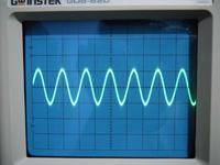
1. Signal at Drain pin 10mV-pk (20mV pk-to-pk) at 1KHz.
2. Mixed Signal at Gate pin 2mV-pk triangular shape riding on around 10Hz signal (LPF frequency).
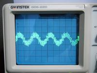
3. Distorted signal seen at Gain and Drain Pin.
4. Max output at 1KHz is limited to 750mV-pk (1.5V pk-pk).
5. Lowering the frequency increases the output voltage.
6. Increasing the frequency decreases the output voltage.


FYI...

Substitutes for 2SK104: BFS70, 2N3821, 2N4220, 2N5359
Substitutes for 2SK105: None

I hope 2N3821, 2N4220, 2N5359 will be available in PSPICE library.

Today, I will perform THD measurement (using PC and RMAA) and will post the results.
 

Hi sameer,
just two comments to the design of the opamp feedback network:

* Error: Rf/Rg=2 should be: Rf/(Rg+Rds)=2
* Why do you use Rds,on in your calculation? Do you operate the FET with VGS=0? I don`t think so.
Didn`t you understand the meaning of the diagram provided with my last posting? The actual Rds must be larger than Rds,on (that is the minimum Rds value).
Note that you can calculate I(DS,S) from Rds,on measurement.
* What is the dc voltage at the gate during operation?

---------- Post added at 12:23 ---------- Previous post was at 11:25 ----------

*One additional question: How did you perform "lowering the frequency"? Variation of one or two components (in parallel)?
*And one additional hint: If you can spend another opamp, there is a WIEN topology (rarely documented) that allows
frequency variation with only ONE resistor (pot).
 
Last edited:

My mistake, It must be Rf/(Rg+Rds)=2

At raw R&D stage:
=============
I thought when the circuit is about to start the voltage at gate pin will be 0 (zero). So, at the initial startup condition resistance formed by JFET would be equal to Rdson. To start the oscillation I used Rdson to calculate the required feedback network resistors. When the oscillation amplitude will build up gradully it will drive the gate voltage from 0V towards negative value which is again limited to one diode [1N4148] drop because the AC-to-DC section (Full-Wave Rectifier and RMS converter) would continue to drive the gate voltage beyond the Pinch Off voltage which will result into oscillation seizour.

Questions:
========
1. Is this a wrong approach ?
2. what is the right approach ?
3. Should I initially set the gate voltage to some negative value and use the Rds for that set point to calculate the feedback network ?

DC at Gate pin:
===========
The DC voltage at the gate during normal operation is -567mV to -571mV.

Lowering or Increasing the frequency:
===========================
There is 10K dual gang potentiometer in WIEN Bridge network. You may clearly see in the snaps and also in the circuit diagram (hand made).

Additional Hint:
===========
The complete circuit is built around one quad-opamp (TL074). I have 2 more quad-opamp (TL074) so I can spend 8 more opamps. Controlling the frequency with single pot would be great for this project.

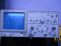
Additional Photographs:
=================
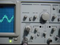
1. Signal at Gate pin + Oscilloscope settings
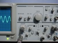
2. Signal at Drain pin + Oscilloscope settings


---------- Post added at 21:38 ---------- Previous post was at 21:26 ----------

Sorry, forgot to tell you the THD figure using ARTA (demo) not RMAA

0.017%
 

I see every thread that posts only 3 other people on where ....???? when I see these forums are very educational. thanks ..:sad::sad:

**broken link removed**
 
Last edited:

The left waveform is apparently indicating an unstable amplitude control loop.
 

FvM: So, How to improve that ?

angel18: Sorry, I could not understand what do you mean to say ?
 

I thought when the circuit is about to start the voltage at gate pin will be 0 (zero). So, at the initial startup condition resistance formed by JFET would be equal to Rdson. To start the oscillation I used Rdson to calculate the required feedback network resistors. When the oscillation amplitude will build up gradully it will drive the gate voltage from 0V towards negative value which is again limited to one diode [1N4148] drop because the AC-to-DC section (Full-Wave Rectifier and RMS converter) would continue to drive the gate voltage beyond the Pinch Off voltage which will result into oscillation seizour.
Questions:
1. Is this a wrong approach ?


No, not "wrong" - but uncommon. See below.

2. what is the right approach ?

Normally, the operating Rs is selected using a curve similar to the one I have shown. This is the best approach because the best Rds region can be selected for optimum regulation. From this starting point all other resistors are calculated.
Since the gate voltage is zero at t=0 the start-up condition is ensured because Rds=RDS,on.


The DC voltage at the gate during normal operation is -567mV to -571mV.


Seems to be a rather good value (app. half the pinch-off votage)

Lowering or Increasing the frequency:
===========================
There is 10K dual gang potentiometer in WIEN Bridge network. You may clearly see in the snaps and also in the circuit diagram (hand made).

In this case, I don`t understand why the oscillation amplitude changes (the opamp gain must remain at G=3).

Additional Hint:
===========
The complete circuit is built around one quad-opamp (TL074). I have 2 more quad-opamp (TL074) so I can spend 8 more opamps. Controlling the frequency with single pot would be great for this project.


Sorry, I forgot to mention that - in this case - no FET regulation is possible (only via anti-parallel diodes across Rf).
The THD value indicates a rather good design. Are you happy with the output amplitude?

---------- Post added at 18:58 ---------- Previous post was at 18:53 ----------

Can you confirm the following readings?
Output: 10 mV,pp at app 3 kHz
Gate control: 10 mV,pp at app 200 Hz?


---------- Post added at 19:02 ---------- Previous post was at 18:58 ----------

The left waveform is apparently indicating an unstable amplitude control loop.

I don`t think that the loop is "unstable" - however, I agree it looks a bit strange. I think it`s the swinging control signal due to the rectification time constant that seems to be to low. I am not sure if the "noisy" signal upon the 200 Hz wave is identical to the 3 kHz osc. signal.
 

I don`t think that the loop is "unstable"
How do you call a control process that maintains steady oscillations otherwise? I just realized, that the frequency seems to be about 50 Hz, so it may be trivial hum as well.
Can you confirm the following readings?
Output: 10 mV,pp at app 3 kHz
Gate control: 10 mV,pp at app 200 Hz?
With both waveforms, the timebase is apparently uncalibrated. If the oscillator is working at 1 kHz, then the control signal is "swinging" at about 50 Hz frequency.
 

If you refer circuit diagram LPF (first order) is configured for 10Hz.

Main Oscillation Frequency: 1KHz
Output frequency from AC-to-DC (Full-wave rectifier): 2 x 1KHz = 2KHz

So the signal at gate should be 2KHz (ripple) riding on 10Hz wave.

Am I correct ?
 

If you refer circuit diagram LPF (first order) is configured for 10Hz.
Main Oscillation Frequency: 1KHz
Output frequency from AC-to-DC (Full-wave rectifier): 2 x 1KHz = 2KHz
So the signal at gate should be 2KHz (ripple) riding on 10Hz wave.
Am I correct ?

Sameer, did you realize the problems connected with a correct interpretation of your photographs? (Calibrated yes/no?).
Therefore, tell us in words how output and control signals look like.
 

A 10 Hz low-pass doesn't necessarily involve a 10 Hz oszillation. But it may be the case, if the control loop's phase margin is insufficient. From the oscilloscope settings, I rather expected 50 or 100 Hz. Why don't you set the var. timebase to "calibrated" and read the frequency from the oscilloscope?
 

Swp. var. (calibrated=no) was adjusted to see the wave otherwise It was shifting.

LvW I have your email ID, FvM please send me your email ID. I'll make video this time so there would be no loop holes.
 

How do you call a control process that maintains steady oscillations otherwise? I just realized, that the frequency seems to be about 50 Hz, so it may be trivial hum as well.
With both waveforms, the timebase is apparently uncalibrated. If the oscillator is working at 1 kHz, then the control signal is "swinging" at about 50 Hz frequency.

Good morning FvM, I know what you mean - and, in principle, I agree. Nevertheless, I am reluctant to call such a loop "unstable", because it is a kind of "instability" which cannot be avoided in a non-linear and discontinuous control loop (caused primarily by the rectification). As you have mentioned: The control signal is "swinging".
LvW
 

Swp. var. (calibrated=no) was adjusted to see the wave otherwise It was shifting.
But you should be able to determine the frequency with sufficient accuracy, and e.g. not have to guess about a frequency of 10 Hz if it's actually 50 - 100.

---------- Post added at 10:25 ---------- Previous post was at 10:14 ----------

I am reluctant to call such a loop "unstable", because it is a kind of "instability" which cannot be avoided in a non-linear and discontinuous control loop (caused primarily by the rectification).

Good morning.
I think, our interpretation of the waveform is still partly different. I assume, that it's a classical linear oscillation, caused by insufficient phase margin of the control loop, and can be avoided. But the question can be easily answered by changing the loop dimensioning (gain and low pass filtering) and must not be decided from a distant desktop.
 

LvW and FvM please ping the below ip address and send me the screenshots. I want to see how much latency is there because I'll provide you the FTP link for videos directly from my PC. Videos are quite large around 250MB each.

IP Address: 202.89.69.35
 

Status
Not open for further replies.

Similar threads

Part and Inventory Search

Welcome to EDABoard.com

Sponsor

Back
Top