Continue to Site

Welcome to EDAboard.com

Welcome to our site! EDAboard.com is an international Electronics Discussion Forum focused on EDA software, circuits, schematics, books, theory, papers, asic, pld, 8051, DSP, Network, RF, Analog Design, PCB, Service Manuals... and a whole lot more! To participate you need to register. Registration is free. Click here to register now.

Crystal oscillator start up spike

FreshmanNewbie

Full Member level 6
Joined
May 10, 2020
Messages
386
Helped
0
Reputation
0
Reaction score
2
Trophy points
18
Activity points
3,857
I have the below waveform for power sequencing of an MPU.

My question is, I am observing the overvoltage as below on the crystal line of 580mV.

Is it OK?

1700215820624.png
 

Attachments

  • 1700215822712.png
    1700215822712.png
    1.2 MB · Views: 53
Hi,

why do you call it OVERvoltage?

I dont see anything weird.
But as with your other threads: without any information about device / datasheet it´s useless to discuss.

It´s like talking about whether shoe size of 8 will fit or not. .... Without knowing the foot size of the person that should wear the shoe.

Klaus
 
I
Hi,

why do you call it OVERvoltage?

I dont see anything weird.
But as with your other threads: without any information about device / datasheet it´s useless to discuss.

It´s like talking about whether shoe size of 8 will fit or not. .... Without knowing the foot size of the person that should wear the shoe.

Klaus
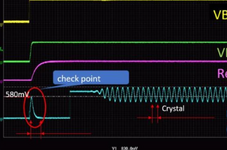
Isn't the initial spike marked in the image of 0.58V wierd?
 
Hi,

no - not at all. I can not find that it is outside any voltage limits nor timing limits.

Indeed such a pulse could be a benefit for a crystal to start up. Some kind of kick start.

Klaus

added:
Don´t get me wrong: I don´t like those guessing games. Several times now I asked for more detail informations. In future I will only respond if there is enough useful information.
 
Typical is crystals have 50 - 100+ microwatt levels max of drive level allowed. So consult
your datasheet. 10's of Mhz kinds of xtals.


Regards, Dana.
 
How much energy do you think was absorbed by the Xtal with that pulse? What is the Spectral Density at the resonant frequency of that pulse vs. a step pulse? Do you know how the Pierce Xtal Oscillator works inside a uC?

CTS says this;
  • "Measurement of crystals also requires drive level to be specified. For better accuracy, lower drive levels are preferred.
  • Drive levels are typically between 10uW to 2mW.
  • Lower-frequency devices with larger quartz wafers can handle higher drive levels without damage.
  • Smaller, higher frequency devices may be damaged by high drive levels, above 5mW.
  • Today’s applications rarely drive acrystal higher than 2mW with typical levels at 100uW maximum.
  • CTS will specify a standard maximum drive level at 100uW, if not defined by a customer.
  • Since the drive level indicates power consumption by the crystal unit while the oscillation circuit works, it is important to keep the crystal within drive level specifications"
More generic Xtal details with power example.
1700281550063.png


Wiki Reference
 
In this link, you can see the below image,

1700464232528.png


Can someone explain why this marked spike is happening ? Is it some phenomenom? Like, crystal gain, negative resistance etc.. ?

I am observing this with a crystal connected to this C21 MCU

I couldn't find much information in the datasheet of the MCU about this crystal spike phenomenon. Any help me?
 
Hi,

just look at the full schematic of an oscillator.
It usually consists of
* inverter
* XTAL
* two cpacitors

Now the situation shows "power up".
At power up both capacitors are considered discharged => 0V
one of these capacitors is at the input of the inverter.

Now the input of the inverter (at power up) is 0V. So what output of the inverter do you expect?
I expect HIGH.
and due to this HIGH ... you get a delayed but rising signal through the XTAL (maybe there is an additional R across the XTAL to ensure proper start up)
inverter output (HIGH) --> C --> XTAL --> C --> inverter input
So the inverter gets a rising signal at the input
and due to this ... I expect the inverter output to fall

I think this is quite expectable. And can be seen in any simulation
I recommend to do such simple simulations on your own. (Mind to switch OFF steady state calculation)
Simulators are easy to use and free, so no excuse not to use them.

(Indeed I´m not a friend of simulators, because the can only calculate as precise as the inputs are. Thus the simple ones don´t care about GND_bounce and PCB layout influence.
But for teaching / learning simple circuit behaviour they are quite useful. No risk for explosions, smoke, smell .. while you can see almost every detail in voltage and current for each single device)

Klaus
 
In this link, you can see the below image,

View attachment 186314

Can someone explain why this marked spike is happening ? Is it some phenomenom? Like, crystal gain, negative resistance etc.. ?

I am observing this with a crystal connected to this C21 MCU

I couldn't find much information in the datasheet of the MCU about this crystal spike phenomenon. Any help me?
All uC ports for ext. osc. have an input and output with an ext. cap to ground on input and an inverter and parallel Megohm for dc self-bias. Thus the input starts at 0 and output pulse to 1 pulling up the input which causes output to sag to 0 until the RC self bias reaches Vdd/2 or whatever the actual threshold is to start oscillating.
 

LaTeX Commands Quick-Menu:

Similar threads

Part and Inventory Search

Welcome to EDABoard.com

Sponsor

Back
Top