Continue to Site

Welcome to EDAboard.com

Welcome to our site! EDAboard.com is an international Electronics Discussion Forum focused on EDA software, circuits, schematics, books, theory, papers, asic, pld, 8051, DSP, Network, RF, Analog Design, PCB, Service Manuals... and a whole lot more! To participate you need to register. Registration is free. Click here to register now.

Benefits of the air gap (PCB slot) to increase the creepage

Status
Not open for further replies.

Lucast85

Member level 3
Joined
Oct 19, 2009
Messages
62
Helped
4
Reputation
8
Reaction score
4
Trophy points
1,288
Location
Italy
Activity points
1,966
Hi everyone,

I've a doubt about the benefits of the air gap to increase the creepage distance between two conductive parts of a component.
I could explain my doubt by using an example with an ethernet transformer.
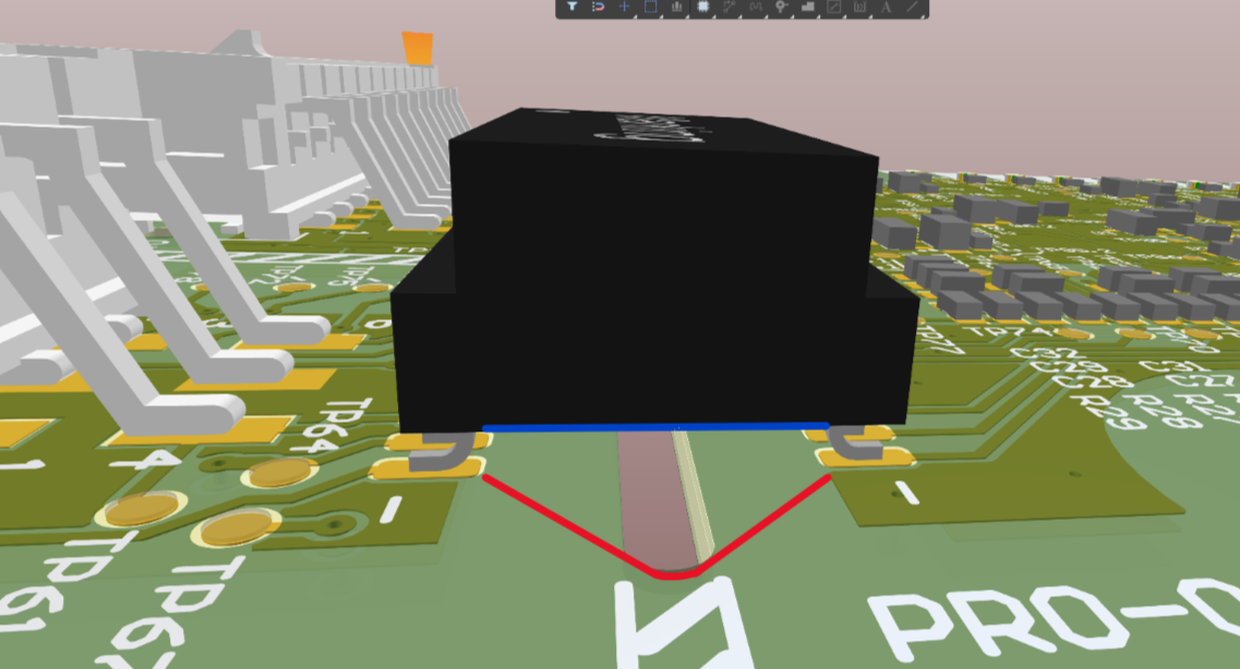
Creepage_ethernet.png

As highligted in the previous image, I suspect it is possible to consider 2 different creepage distances:
  • In blue the creepage along the componet's surface itself (in the back side of the transformer) that is the minimum distance between the pins (conductive parte to be isolated) of the componets;
  • In red the creepage along the PCB's surface that is the distance between the pads on the PCB;
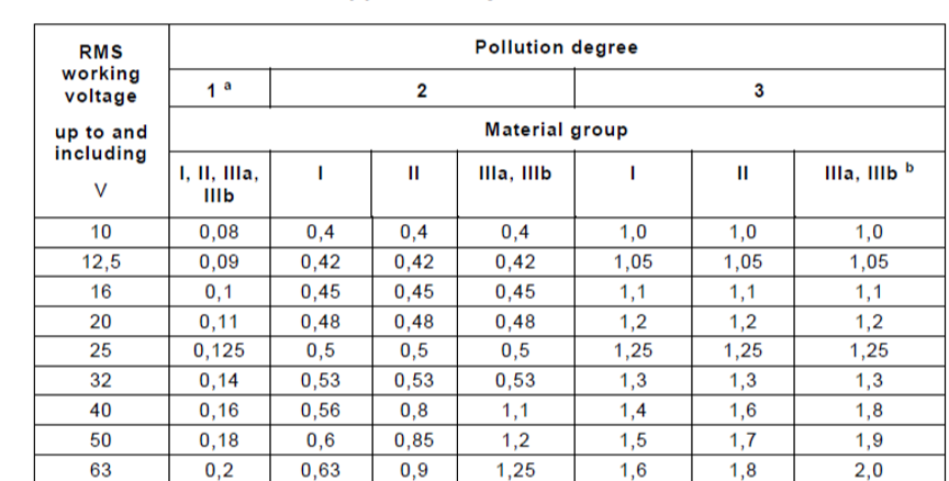
Obviously, to be compliant with the normative, the twos must be higher than the value expressed into the tables of the normatives. The following table is just an example of the creepage distances in mm, as reported into the normative:
creepageTable.png

My observations are the following:
  • With the air-gap (PCB slot) I can increase the creepage distance along the PCB surface (red line in the previous image), but the creepage along the component's pins (blue line) remains inalterated, thus:
    1. If the considered pollution degree is 1, then the air gap is almost unuseful because all the material group (PCB material e.g. FR4 and transformer material) are grouped into the same column. This means that the min. creepage distances along the PCB and along the component's surface (two different materials) must be the same. In this case, the pins spacing is critical.
    2. If the considered pollution degree is 2 or 3, then the air gap is useful because the crepage distance to be considered could be splitted in two: the creepage along the surface of the component that is frequently better than material group III and the creepage along the PCB that is usually material group III. In this case, along the PCB, I can reach the creepage prescribed by the normative (usually higher than the creepage distance prescrived along the component surface) by using the slot.
    3. If the considered pollution degree is 2 or 3, and the material group of the PCB and the material group of the component are the same, then the situation is the same of the point 1.
It make sense?
Thanks,
 

Solution
I don't understand your approach. You already know that slots can increase creepage pathes in some cases. They are particularly useful when component package has better CTI than PCB.

What's the purpose of constructing cases where slots are not useful? Better analyse the actual conditions of your design. If you have questions about it, please ask.

I generally doubt that PD 1 applies to your designs, the prerequisites are rarely met.
as i understand your chart, the largest distance is 2 mm
how far apart are the legs of your transformer?

the only time i worried about creepage was in high voltage
transformer output - three series-ed secondaries producing 10,000 volt.
we cut all the way through the board, so any arc would have to
go through the insulating oil. it solved our problem.

ethernet does not carry sufficient voltage or power to arc.
i expect the transformer you are discussing is about 5 mm across
much greater than the 2 mm worst case in the chart

clean the board and conformal coat it
no worries.
 

My doubt is not about the specific application shown in the image but is a general doubt/observation. The table is just an example to show the difference between the second column (the one that grouped all the material groups and the other column on the right that make differences between material groups).

I'm currently designing a system at 1400V that uses 1500V mosfets, optocoupler, etc. It uses ethernet-like transformer but the signal is not ethernet and must be isolated for 1500V.

My doubt is about the usefulness of the PCB slot. In my opinion, if I work with a pollution degree 1, the PCB slot is not very useful because it is the creepage along the surface of the component itself that limits the max. voltage.
Are the considerations of the point 1,2 and 3 correct in you opinion?
 

I don't understand your approach. You already know that slots can increase creepage pathes in some cases. They are particularly useful when component package has better CTI than PCB.

What's the purpose of constructing cases where slots are not useful? Better analyse the actual conditions of your design. If you have questions about it, please ask.

I generally doubt that PD 1 applies to your designs, the prerequisites are rarely met.
 
Solution
Hi FvM,
thanks for the reply.
Probably I exposed my doubt with the wrong words...I wan't costruct cases where slot are not useful. I just want to undertand which are the cases where the slot could help and which are the cases where the slot is unuseful.
However with your response:
They are particularly useful when component package has better CTI than PCB.
you give me the confirm that the slot is really useful only if the CTI between PCB and package is different.

Other doubts are about the PD. I read about the different definition of PD in the normatives but I cannot find how can I reach such situations; e.g., for PD1:
No pollution or only dry, nonconductive pollution occurs. The pollution has no effect.
Can I reach PD1 by using only an IP6x enclosure? There exists some relations between IP6x degree-enclousure and Pollution degree? Which are the test involved?
 

According to IEC 61010, PD 1 can be only achived with IP6x enclosure if installation and maintenance is carried out in controlled enviroment, means temperature 5 °C to 40 °C and maximum relative humidity 80 % for temperatures up to 31 °C decreasing linearly to 50 % relative humidity at 40 °C. Also outer PD must higher than 2. Not sure if it can be achieved for your instrument.

Conformal coating might be the easier way if you rely on PD 1.

1638807986068.png
 
Thank you FvM,
I was looking for this table from time.

So, as you suggest the only way is to use conformal coating. According to the IEC 62368-1 I have to consider the table G13 and, if the voltage is >455Vpeak, I need to perform some test (G13.6 of IEC 62368-1) on the coating.
G13.png

Is it correct?
 

Status
Not open for further replies.

Part and Inventory Search

Welcome to EDABoard.com

Sponsor

Back
Top