Continue to Site

Welcome to EDAboard.com

Welcome to our site! EDAboard.com is an international Electronics Discussion Forum focused on EDA software, circuits, schematics, books, theory, papers, asic, pld, 8051, DSP, Network, RF, Analog Design, PCB, Service Manuals... and a whole lot more! To participate you need to register. Registration is free. Click here to register now.

Back to back MOSFET configuration

mirror_pole

Member level 3
Joined
Nov 22, 2020
Messages
56
Helped
0
Reputation
0
Reaction score
2
Trophy points
8
Activity points
554
Hello guys,

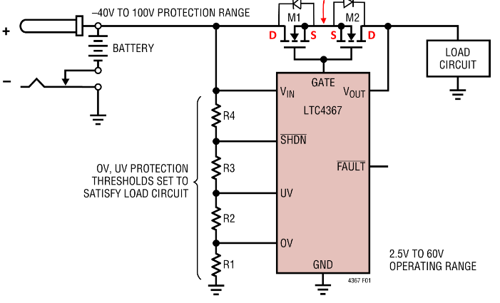
I have a question about the working mechanism of a back to back MOSFET configuration. I just dont understand how this setup which is used as a bidirectional switch works. If i take this Ic for example i assume that my max voltage potential at the common source terminal is equal to Vs=Vout+Vf with Vf being the forward voltage of M2 body diode. So to turn on both FETs Vgs>Vth => Vg>Vth+Vout+Vf is needed. But what about the Vds? In case of M1 if i apply an input voltage greater then the source potential it will conduct, but what about M2? From my understanding the current is flowing from drain to source but in the case of M2 it is "reverse biased", so how is M2 even able to conduct? Through the body diode of M2?
b2b.PNG
 
Last edited:
Reverse biased FET drops body diode forward voltage in off-state. On-resistance is similar (few milliohms) with forward and reversed Vds, review FET datsheets.
 
Hi,

In other words:
* when MOSFET is OFF, then current flow is only in one direction through diode
* when MOSFET is ON, then current flow in both directions, with low R_DS_ON, means not via diode.

Klaus
 
Thank you for the answers. But does it mean that M2 conducts through the channel or the body diode? Because here (https://www.homemade-circuits.com/bidirectional-switch/) it says that one of the MOSFET conducts through the channel and the other through its diode. In some other posts i saw people saying that both transistors conduct through the channel, which i dont understand since i thought that conducting through the channel is only possible from drain to source.
 
Hi,

As already written: (true for every Mosfet)
* when MOSFET is OFF, then current flow is only in one direction through diode
* when MOSFET is ON, then current flow in both directions, with low R_DS_ON, means not via diode.
The same applies for M2.

So when GATE output of the shown IC is LOW, then both MOSFETs are ON.
And again: this means no current flow through body diode.

Only at the very beginning
* you may have the load side of M2 to be 0V...
* thus, when GATE is 0V then M1 becomes ON, M2 still OFF (V_DS too low due to zero Drain voltage)
--> current flow through Diode of M2
--> automatically M2 Drain voltage rises, thus V_DS rises
--> M2 immediately goes ON, too
--> no diode current flow anymore

Klaus

Added: I recommend you to use a simulation software ... it tells you what happens
 
Thank you Klaus, i think i got it now. I made the mistake to assume that current can only flow from drain to source, but as you said only at the very beginning current flows through the diode of M2. As soon as the output gets "charged up" VDS rises and therefore M2 turns on =>M1 and M2 conduct through the channel.
 

LaTeX Commands Quick-Menu:

Similar threads

Part and Inventory Search

Welcome to EDABoard.com

Sponsor

Back
Top