happsky
Advanced Member level 4
I have a metal between 3 oixde layers, show as bellow:

I face 3 problems as :
1. the metal is thicker than oxide layer ,this will calls error;
2.And then,I split the metal to 3 metal layers ,and make them overlay as a metal layer . The thickness of center layer is eqeul to oxide2, this also forbidden.
3. Follow step 2 's idea, I change the center metal to be a vias ,and it no error now. But I don't know if a vias is equal to a metal when meshing and simulation( I have set the vias to be 3D-mesh the same as the metal layer before simulation).
note:the version of ads is 2011
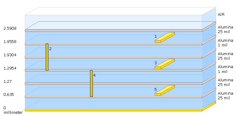
using step 3 's idea the substrate is shown as:

And do I need to set the precedence of the metal layer when they overlay?
Any ideas? thank you very much!
I face 3 problems as :
1. the metal is thicker than oxide layer ,this will calls error;
2.And then,I split the metal to 3 metal layers ,and make them overlay as a metal layer . The thickness of center layer is eqeul to oxide2, this also forbidden.
3. Follow step 2 's idea, I change the center metal to be a vias ,and it no error now. But I don't know if a vias is equal to a metal when meshing and simulation( I have set the vias to be 3D-mesh the same as the metal layer before simulation).
note:the version of ads is 2011
using step 3 's idea the substrate is shown as:
And do I need to set the precedence of the metal layer when they overlay?
Any ideas? thank you very much!
Last edited: