druiz
Newbie
Hello,
I am doing 2 EM co-simulations in ADS for a simple OMN. One of the simulations is with the extracted S2 parameters and the other is placing the component of the library from ADS: "sc_atc_100_CDR13BG_G_19960828". The S2 parameters has been extracted trought "SPOutput" in magnitude and phase from "sc_atc_100_CDR13BG_G_19960828" component. The ports to extract de S2 parameters are 50 Ohms in 1 and 2. In the other hand, to validate the EM co-simulation, I am doing a schematic simulation of the same OMN and comparing the 3 simulations. The obtanied results and the layouts used are:
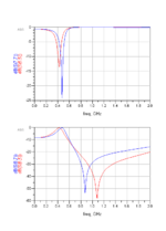
Simulation obtained with S parameters and S2P_Pad3

Simulation obtained with component
sc_atc_100_CDR13BG_G_19960828 placing in the layout

Layout for EM co- simulation with S2P_Pad3

Layout for EM co- simulation with
sc_atc_100_CDR13BG_G_19960828 component placed

Blue lines in S parameters graph are the EM co-simulation and red lines are the schematic simulation. As how can see, the simulation with the component "sc_atc_100_CDR13BG_G_19960828" differs a lot in relation to the schematic simulation and the S2P_Pad3 component, and the simulation with S parameters and S2P_Pad3 is closer to the schematic simulation than the simulation with the component.
Why this happens, if the S parameters in the SP3-Pad has been extracted from the component "sc_atc_100_CDR13BG_G_19960828"? I think in the case of the component instead of the S parameters with S2P_Pad, the EM co-simulation has considering the encapsulation of the component but not in the case of the S2P_Pad component, where the only reflected are the pad's size.
Whic one should be the correct simulation for an EM co-simulation and is this the right way to do it?
I am doing 2 EM co-simulations in ADS for a simple OMN. One of the simulations is with the extracted S2 parameters and the other is placing the component of the library from ADS: "sc_atc_100_CDR13BG_G_19960828". The S2 parameters has been extracted trought "SPOutput" in magnitude and phase from "sc_atc_100_CDR13BG_G_19960828" component. The ports to extract de S2 parameters are 50 Ohms in 1 and 2. In the other hand, to validate the EM co-simulation, I am doing a schematic simulation of the same OMN and comparing the 3 simulations. The obtanied results and the layouts used are:
Simulation obtained with S parameters and S2P_Pad3
Simulation obtained with component
sc_atc_100_CDR13BG_G_19960828 placing in the layout
Layout for EM co- simulation with S2P_Pad3
Layout for EM co- simulation with
sc_atc_100_CDR13BG_G_19960828 component placed
Blue lines in S parameters graph are the EM co-simulation and red lines are the schematic simulation. As how can see, the simulation with the component "sc_atc_100_CDR13BG_G_19960828" differs a lot in relation to the schematic simulation and the S2P_Pad3 component, and the simulation with S parameters and S2P_Pad3 is closer to the schematic simulation than the simulation with the component.
Why this happens, if the S parameters in the SP3-Pad has been extracted from the component "sc_atc_100_CDR13BG_G_19960828"? I think in the case of the component instead of the S parameters with S2P_Pad, the EM co-simulation has considering the encapsulation of the component but not in the case of the S2P_Pad component, where the only reflected are the pad's size.
Whic one should be the correct simulation for an EM co-simulation and is this the right way to do it?