wandola
Junior Member level 3
Hi guys,
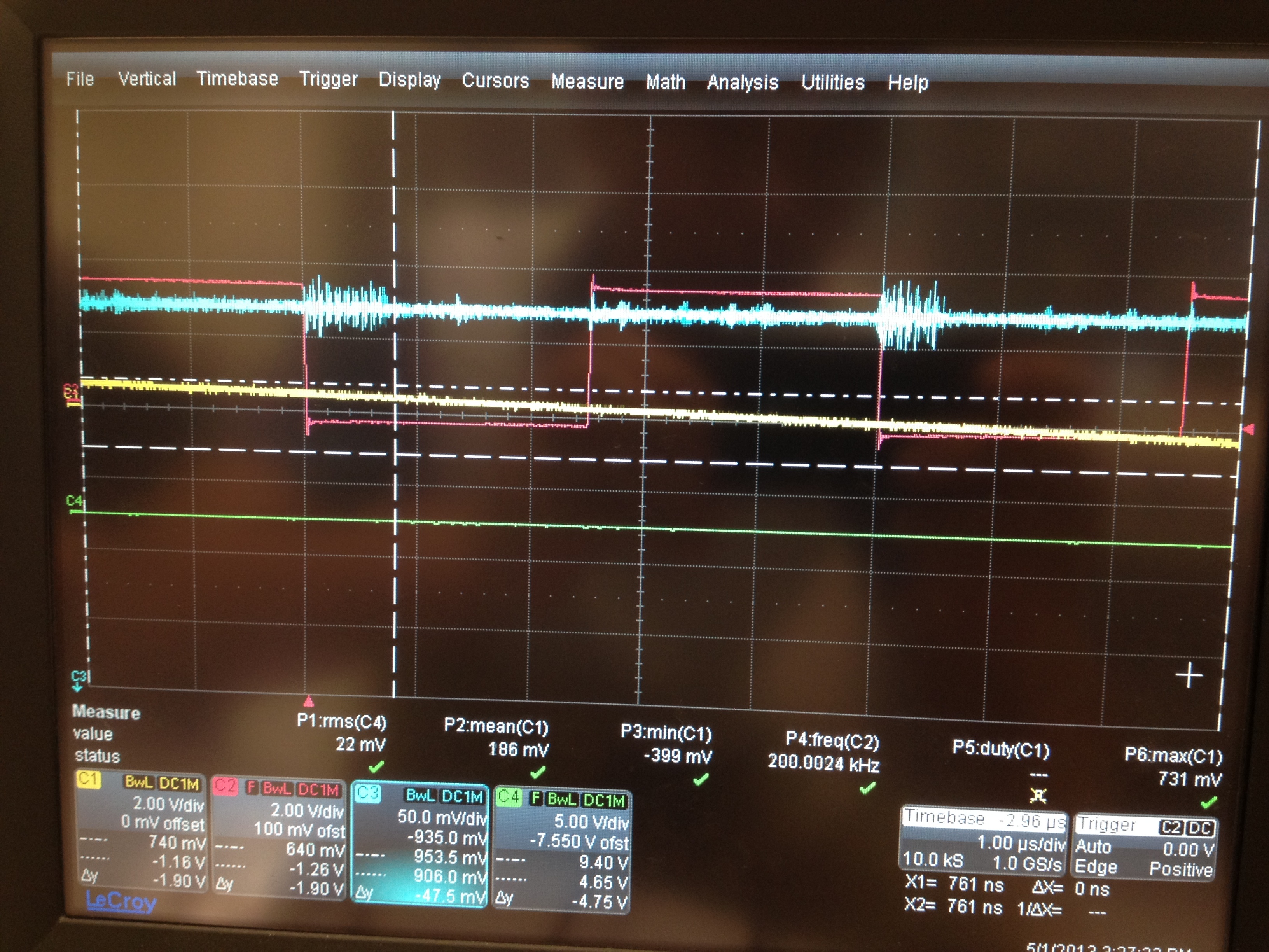
I have designed a low-speed SAR ADC in a 65nm CMOS. sampling speed 1MS/s. The internal clock signal was about 5MHz.
When I conduct the measurement, I found that the VDD (VDDAana, VDDdig, and VREF are all connected to the same PAD to 1.0V) changes for about 100 mV during ADC conversion.
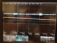
the blue line is the VDD.
This is my second chip and I found this problem again.
Can any expert give me some opinions?? Is this normal??
thnks a lot.
I have designed a low-speed SAR ADC in a 65nm CMOS. sampling speed 1MS/s. The internal clock signal was about 5MHz.
When I conduct the measurement, I found that the VDD (VDDAana, VDDdig, and VREF are all connected to the same PAD to 1.0V) changes for about 100 mV during ADC conversion.
the blue line is the VDD.
This is my second chip and I found this problem again.
Can any expert give me some opinions?? Is this normal??
thnks a lot.